TLD7002-16ES
Datasheet
7 Load Diagnostic
7
Load Diagnostic
Features
7.1
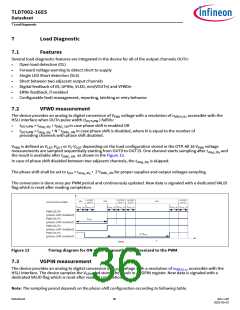
Several load diagnostic features are integrated in the device for all of the output channels OUTn:
•
•
•
•
•
•
•
Open load detection (OL)
Forward voltage warning to detect short to supply
Single LED Short detection (SLS)
Short between two adjacent output channels
Digital feedback of VS, GPINn, VLED, min(VOUTn) and VFWDn
ERRn feedback, if enabled
Configurable fault management, reporting, latching or retry behavior
7.2
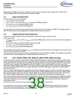
VFWD measurement
The device provides an analog to digital conversion of VFWD voltage with a resolution of nVRES,Hi, accessible with the
HSLI interface when OUTn pulse width (tOUTnPW ) fulfills:
•
•
tOUTnPW > tdiag_dly + tDIAG_ON in case phase shif is enabled OR
tOUTnPW > tdiag_dly + N * tDIAG_ON in case phase shif is disabled, where N is equal to the number of
preceding channels with phase shif disabled.
VFWD is defined as VLED-VOUT or VS-VOUT depending on the load configuration stored in the OTP. All 16 VFWD voltage
measurements are sampled sequentially starting from OUT0 to OUT15. One channel starts sampling afer tdiag_dly and
the result is available afer tDIAG_ON as shown in the Figure 13.
In case of phase shif disabled between two adjacent channels, the tdiag_dly is skipped.
The phase shif shall be set to tphs > tdiag_dly + 2*tDIAG_ON for proper supplies and output voltages sampling.
The conversion is done once per PWM period and continuously updated. New data is signaled with a dedicated VALID
flag which is reset afer reading completion.
Figure 13
Timing diagram for ON-state diagnostics synchronized to the PWM
7.3
VGPIN measurement
The device provides an analog to digital conversion of VGPIN voltage with a resolution of nVRES,Lo, accessible with the
HSLI interface. The device samples the VGPIn and stores the result in a VGPIN register. New data is signaled with a
dedicated VALID flag which is reset afer reading completion.
Note: The sampling period depends on the phase-shif configuration according to following table.
Datasheet
36
Rev.1.00
2022-05-03

 INFINEON [ Infineon ]