TLD7002-16ES
Datasheet
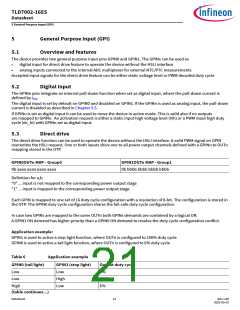
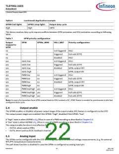
5 General Purpose Input (GPI)
The GPIN ADC measurement is described in Chapter 7.3.
5.6
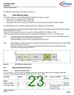
GPIN PWM decoding
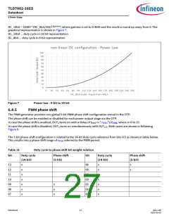
The GPINs can decode an input PWM signal with a frequency of fPWM_GPINn where
•
•
•
a duty cycle dcLO is detected as OFF activation OR
a duty cycle dcHI is detected as ON activation OR
a duty cycle outbound of dcLO OR dcHI is detected as fault and reported via the HSLI interface or ERRn.
The GPIN decoding can be enabled or disabled via the OTP configuration for each GPINn.
In case of active mode the GPIN warning flag (GPINn_WRN) is reported via the HSLI output status byte OR activating
ERRN with a PWM.DC = 100ꢀ.
In case of fail-safe mode the fault state is reported by activating ERRN with a PWM.DC = 100ꢀ.
A GPIN warning on ERRN is reported, when fault management configuration is set to "0" - no state change.
Note:
Note:
The device interprets an immediate warning recovery as OFF activation. At least two GPIN PWM periods are
required to detect an ON activation afeꢀ a GPIN warning.
The GPIN_WRN flag is cleared with an explicit HWCR frame from LCU.
If both GPINs are used for direct control and GPIN decoding enabled a phase shif between 10 µs and 1/fPWM
and same frequency are required.
If the phase shif constraint is not granted, a GPIN short (GPIN_SHORT) is detected by the device and
reported in the output status byte FAULT bit.
Figure 6
GPIN PWM decoding scheme
5.7
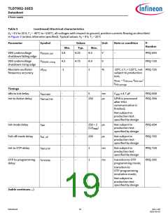
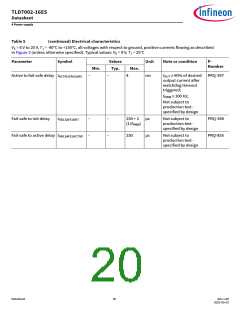
Electrical characteristics
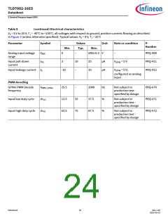
Table 8
Electrical characteristics
VS = 6 V to 20 V, TJ = -40°C to +150°C, all voltages with respect to ground, positive currents flowing as described
in Figure 2 (unless otherwise specified). Typical values: VS = 9 V, TJ = 25°C
Parameter
Symbol
Values
Typ.
Unit
Note or condition
P-
Number
Min.
Max.
GPINn
Input low voltage
Input high voltage
VIL
0
–
0.8
5.5
V
V
–
PRQ-407
VIH
2.0
–
Internally clamped to PRQ-408
5.5 V if the input
current is ≤ IGPINn
(table continues...)
Datasheet
23
Rev.1.00
2022-05-03

 INFINEON [ Infineon ]