TDA 5210
preliminary
Reference
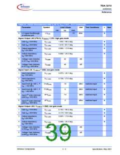
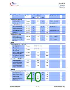
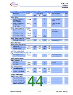
Table 5-3 AC/DC Characteristics with TA 25 °C, VVCC = 4.5 ... 5.5 V (continued)
Parameter
Symbol
Limit Values
Unit
Test Conditions
L
Item
min
typ
max
Signal 3VOUT (PIN 24)
1
2
Output voltage
Current out
V
2.9
-3
3.1
-5
3.3
-10
V
3VOUT Pin open
see Section 4.1
3VOUT
I
µA
3VOUT
Signal THRES (PIN 23)
1
2
3
4
Input Voltage range
LNA low gain mode
LNA high gain mode
Current in
V
0
0
V -1V
S
V
V
see Section 4.1
THRES
V
THRES
V
2.8
3
5
V
S
V
or shorted to Pin 24
THRES
ITHRES_in
nA
Signal TAGC (PIN 4)
1
Current out,
LNA low gain state
ITAGC_out
-3.6
1
-4.2
1.6
-5
µA
µA
RSSI > V
RSSI>V
THRES
2
Current in, LNA high
gain state
V
2.2
TAGC_in
THRES
MIXER
Signal Input MI/MIX (PINS 8/9)
ꢀ
ꢀ
ꢀ
1
2
3
Input impedance,
=434 MHz
S
S
0.942 / -14.4 deg
0.918 / -28.1 deg
-28
11 MIX
f
RF
Input impedance,
=869 MHz
11 MIX
f
RF
Input 3rd order intercept
MIX
MIX
IIP3
IIP3
dBm
dBm
point f =434 MHz
RF
Input 3rd order intercept
ꢀ
ꢀ
4
-26
point f =869 MHz
RF
Signal Output IFO (PIN 12)
1
2
Output impedance
Z
330
+19
Ω
IFO
Conversion Voltage
G
dB
MIX
Gain f =434 MHz
RF
3
Conversion Voltage
G
+18
dB
MIX
Gain f =869 MHz
RF
LIMITER
Signal Input LIM/X (PINS 17/18)
ꢀ
1
2
3
4
Input Impedance
RSSI dynamic range
RSSI linearity
Z
264
60
330
396
Ω
dB
LIM
DR
80
RSSI
ꢀ
ꢀ
LIN
f
dB
±1
RSSI
Operating frequency
(3dB points)
5
10.7
23
MHz
LIM
Wireless Components
5 - 6
Specification, May 2001

 INFINEON [ Infineon ]