TDA 5210
preliminary
Reference
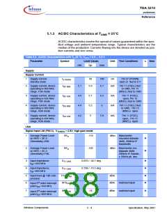
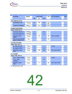
5.1.3 AC/DC Characteristics at TAMB = 25°C
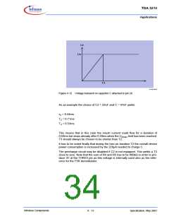
AC/DC characteristics involve the spread of values guaranteed within the spec-
ified voltage and ambient temperature range. Typical characteristics are the
median of the production. Currents flowing into the device are denoted as pos-
itive currents and vice versa.
Table 5-3 AC/DC Characteristics with TA 25 °C, VVCC = 4.5 ... 5.5 V
Parameter
Symbol
Limit Values
Unit
Test Conditions
L
Item
min
typ
max
Supply
Supply Current
1
Supply current,
standby mode
IS PDWN
50
100
6.7
nA
Pin 27 (PDWN)
open or tied to 0 V
2
Supply current, device
operating in 868 MHz
range, FSK mode
I
5.1
4.9
4.4
5.9
mA
Pin 11 (FSEL) tied
to GND, Pin 15
(MSEL) tied to GND
SF 868
3
4
Supply current, device
operating in 434 MHz
range, FSK mode
I
5.7
5.2
6.5
6
mA
mA
Pin 11 (FSEL)
open, Pin 15
(MSEL) tied to GND
SF 434
Supply current, device
operating in 868 MHz
range, ASK mode
I
I
Pin 11 (FSEL) tied
to GND, Pin 15
(MSEL) open
SA 868
SA 434
5
Supply current, device
operating in 434 MHz
range, ASK mode
4.2
5
5.8
mA
Pin 11 (FSEL)
open, Pin 15
(MSEL) open
LNA
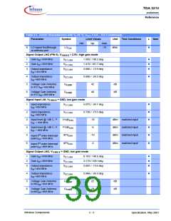
Signal Input LNI (PIN 3), V
> 2.8V, high gain mode
THRES
1
Average Power Level
at BER = 2E-3
(Sensitivity) ASK
RFin
-110
dBm Manchester
encoded datarate
ꢀ
ꢀ
4kBit, 280kHz IF
Bandwidth
2
Average Power Level
at BER = 2E-3
RFin
-103
dBm Manchester enc.
datarate 4kBit,
(Sensitivity) FSK
280kHz IF Bandw.,
± 50kHz pk. dev.
ꢀ
ꢀ
3
4
Input impedance,
S
S
0.873 / -34.7 deg
0.738 / -73.5 deg
11 LNA
f
=434 MHz
RF
Input impedance,
=869 MHz
11 LNA
f
RF
ꢀ
ꢀ
5
6
Input level @ 1dB com-
pression
P1dB
IIP3
-15
-10
dBm
LNA
Input 3rd order intercept
LNA
LNA
dBm
dBm
matched input
matched input
point f =434 MHz
RF
Input 3rd order intercept
ꢀ
7
IIP3
-14
point f =869 MHz
RF
Wireless Components
5 - 4
Specification, May 2001

 INFINEON [ Infineon ]