TDA 5210
preliminary
Reference
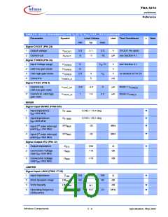
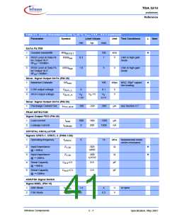
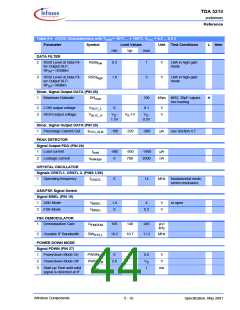
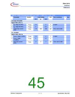
Table 5-3 AC/DC Characteristics with TA 25 °C, VVCC = 4.5 ... 5.5 V (continued)
Parameter
Symbol
Limit Values
Unit
Test Conditions
L
Item
min
typ
max
DATA FILTER
ꢀ
1
2
Useable bandwidth
BW
100
1
kHz
V
BB FILT
RSSI Level at Data Fil-
ter Output SLP,
RSSI
0.3
1.8
LNA in high gain
mode
low
RF =-103dBm
IN
3
RSSI Level at Data Fil-
ter Output SLP,
RSSI
3
V
LNA in high gain
mode
high
RF =-30dBm
IN
Slicer, Signal Output DATA (PIN 25)
ꢀ
1
Maximum Datarate
DR
100
0.1
kBps NRZ, 20pF capaci-
tive loading
max
2
3
LOW output voltage
HIGH output voltage
V
V
0
V
V
SLIC_L
V -
S
V -1V
S
V -
S
SLIC_H
1.3V
-100
0.7V
-300
Slicer, Signal Output DATA (PIN 20)
Precharge Current Out
1
I
-220
µA
see Section 4.7
PCH_SLN
PEAK DETECTOR
Signal Output PDO (PIN 26)
1
2
Load current
I
-600
0
-950
200
-1300
1000
µA
nA
load
Leakage current
I
leakage
CRYSTAL OSCILLATOR
Signals CRSTL1, CRSTL 2, (PINS 1/28)
1
Operating frequency
f
6
14
MHz fundamental mode,
series resonance
CRSTL
ꢀ
ꢀ
2
Input Impedance
@ ~6MHz
Z
-825
+j695
Ω
1-28
3
4
5
Input Impedance
@ ~13MHz
Z
-600
+j1010
Ω
1-28
Serial Capacity
@ ~6MHz
C
C
=C1
8.9
pF
pF
S 6
Serial Capacity
@ ~13MHz
=C1
5.9
S13
ASK/FSK Signal Switch
Signal MSEL (PIN 15)
1
2
ASK Mode
FSK Mode
V
1.4
0
4
V
V
or open
MSEL
V
0.2
MSEL
Wireless Components
5 - 7
Specification, May 2001

 INFINEON [ Infineon ]