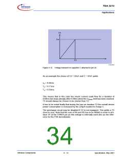
TDA 5210
preliminary
Reference
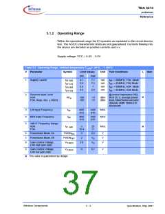
5.1.2 Operating Range
Within the operational range the IC operates as explained in the circuit descrip-
tion. The AC/DC characteristic limits are not guaranteed. Currents flowing into
the device are denoted as positive currents and v.v.
Supply voltage: VCC = 4.5V .. 5.5V
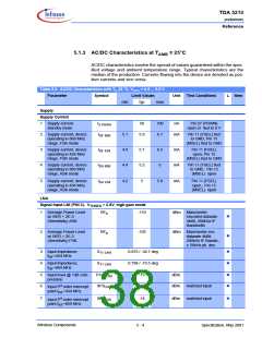
Table 5-2 Operating Range, Ambient temperature T
= -40°C ... + 105°C
AMB
#
Parameter
Symbol
Limit Values
Unit
Test Conditions
L
Item
min
max
1
Supply Current
I
4.1
3.9
3.4
3.2
7.7
7.5
7
mA
mA
mA
mA
f
f
f
f
= 868MHz, FSK Mode
= 434MHz, FSK Mode
= 868MHz, ASK Mode
= 434MHz, ASK Mode
SF 868
RF
RF
RF
RF
I
SF 434
I
SA 868
6.8
I
SA 434
2
Receiver Input Level
ASK
FSK, frequ. dev. ± 50kHz
@ source impedance 50Ω,
BER 2E-3, average power
level, Manchester encoded
datarate 4kBit, 280kHz IF
Bandwidth
ꢀ
RFin
-106
-100
-13
-13
dBm
dBm
3
4
5
LNI Input Frequency
MI/X Input Frequency
fRF
fMI
400/
810
440/
870
MHz
MHz
400/
810
440/
870
3dB IF Frequency Range
ASK
FSK
fIF -3dB
5
10.4
23
11
MHz
ꢀ
6
7
8
Powerdown Mode On
Powerdown Mode Off
PWDNON
PWDNOFF
VTHRES
0
2
0.8
V
V
V
V
S
S
Gain Control Voltage,
LNA high gain state
2.8
V
9
Gain Control Voltage,
LNA low gain state
VTHRES
0
0.7
V
ꢀꢀ This value is guaranteed by design.
Wireless Components
5 - 3
Specification, May 2001

 INFINEON [ Infineon ]