TDA 5210
Functional Description
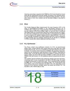
3.4.4 Crystal Oscillator
The on-chip crystal oscillator circuitry allows for utilisation of quartzes both in
the 6 and 13MHz range as the overall division ratio of the PLL can be switched
between 64 and 128 via the CSEL (Pin 16) pin according to the following table.
Table 3-3 CSEL Pin Operating States
CSEL
Crystal Frequency
6.xx MHz
Open
Shorted to ground
13.xx MHz
The calculation of the value of the necessary quartz load capacitance is shown
in Section 4.3, the quartz frequency calculation is explained in Section 4.4.
3.4.5 Limiter
The Limiter is an AC coupled multistage amplifier with a cumulative gain of
approximately 80 dB that has a bandpass-characteristic centred around
10.7 MHz. It has a typical input impedance of 330 Ω to allow for easy interfacing
to a 10.7 MHz ceramic IF filter. The limiter circuit also acts as a Receive Signal
Strength Indicator (RSSI) generator which produces a DC voltage that is
directly proportional to the input signal level as can be seen in Figure 4-2. This
signal is used to demodulate ASK-modulated receive signals in the subsequent
baseband circuitry. The RSSI output is applied to the modulation format switch,
to the Peak Detector input and to the AGC circuitry.
In order to demodulate ASK signals the MSEL pin has to be left open as
described in the next chapter.
3.4.6 FSK Demodulator
To demodulate frequency shift keyed (FSK) signals a PLL circuit is used that is
contained fully on chip. The Limiter output differential signal is fed to the linear
phase detector as is the output of the 10.7 MHz center frequency VCO. The
demodulator gain is typically 140µV/kHz. The passive loop filter output that is
comprised fully on chip is fed to both the VCO and the modulation format switch
described in more detail below. This signal is representing the demodulated sig-
nal with high frequencies applied to the demodulator demodulated to logic ones
and low frequencies demodulated to logic zeroes. Please note that due to this
behaviour a sign inversion of the data occurs in case of high-side injection of
the local oscillator at receive frequencies below 840 or 420MHz, respectively.
See also .
The modulation format switch is actually a switchable amplifier with an AC gain
of 11 that is controlled by the MSEL pin (Pin 15) as shown in the following table.
This gain was chosen to facilitate detection in the subsequent circuits. The DC
Wireless Components
3 - 11
Specification, May 2001

 INFINEON [ Infineon ]