TDA 5210
Functional Description
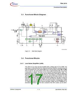
3.3 Functional Block Diagram
VCC
IF
Filter
MSEL
LNO
MI
MIX IFO
12
LIM
LIMX
18
FFB
OPP
SLP
SLN
20
6
8
9
17
15
21
19
22
LNI
3
4
LNA
RF
-
+
-
FSK
PLL Demod
-
DATA
25
FSK
ASK
+
LIMITER
SLICER
+
OP
-
+
TAGC
PEAK
DETECTOR
26 PDO
TDA 5210
OTA
THRES
23
24
UREF
3VOUT
AGC
Reference
Φ
DET
CRYSTAL
OSC
: 1 / 2
VCO
: 128 / 64
VCC
14
13
Bandgap
Reference
Loop
Filter
DGND
16
1
28
27
11
2,7
5,10
PDWN
VCC AGND
FSEL
CSEL
Crystal
Function_5200.wmf
Figure 3-2
Main Block Diagram
3.4 Functional Blocks
3.4.1 Low Noise Amplifier (LNA)
The LNA is an on-chip cascode amplifier with a voltage gain of 15 to 20dB. The
gain figure is determined by the external matching networks situated ahead of
LNA and between the LNA output LNO (Pin 6) and the Mixer Inputs MI and MIX
(Pins 8 and 9). The noise figure of the LNA is approximately 3dB, the current
consumption is 500µA. The gain can be reduced by approximately 18dB. The
switching point of this AGC action can be determined externally by applying a
threshold voltage at the THRES pin (Pin 23). This voltage is compared internally
with the received signal (RSSI) level generated by the limiter circuitry. In case
that the RSSI level is higher than the threshold voltage the LNA gain is reduced
and vice versa. The threshold voltage can be generated by attaching a voltage
divider between the 3VOUT pin (Pin 24) which provides a temperature stable
3V output generated from the internal bandgap voltage and the THRES pin as
described in Section 4.1. The time constant of the AGC action can be deter-
Wireless Components
3 - 9
Specification, May 2001

 INFINEON [ Infineon ]