TC1796
Functional Description
VFAREF VDDAF VDDMF
VFAGND VSSAF
VSSMF
fFADC
fCLC
Clock
Control
FAIN0P
FAIN0N
FAIN1P
FAIN1N
FAIN2P
FAIN2N
FAIN3P
FAIN3N
AN24
AN25
AN26
AN27
AN28
AN29
AN30
AN31
D
D
D
D
D
D
D
D
Address
Decoder
FADC
Module
Kernel
SR[3:0]
Interrupt
Control
To DMA
OUT1
OUT9
OUT18
OUT26
OUT2
OUT10
OUT19
OUT27
P1.0 / REQ0
P1.1 / REQ1
P7.0 / REQ4
P7.1 / REQ5
A1
A1
A1
A1
GPTA0
GS[7:0]
TS[7:0]
PDOUT2
PDOUT3
External Request Unit
(SCU)
MCA06053
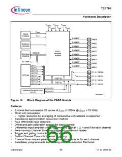
Figure 16
Features
Block Diagram of the FADC Module
•
•
Extreme fast conversion: 21 cycles of fFADC (= 280ns @ fFADC = 75 MHz)
10-bit A/D conversion
– Higher resolution by averaging of consecutive conversions is supported
Successive approximation conversion method
Four differential input channels
•
•
•
•
•
•
•
•
•
Offset and gain calibration support for each channel
Differential input amplifier with programmable gain of 1, 2, 4 and 8 for each channel
Free-running (Channel Timers) or triggered conversion modes
Trigger and gating control for external signals
Built-in Channel Timers for internal triggering
Channel timer request periods independently selectable for each channel
Selectable, programmable anti aliasing and data reduction filter block
Data Sheet
66
V1.0, 2008-04

 INFINEON [ Infineon ]