TC1796
Functional Description
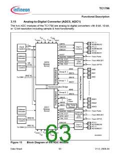
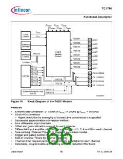
The A/D converters operate by the method of the successive approximation. A
multiplexer selects between up to 32 analog inputs that can be connected with the 16
conversion channels in each ADC module. An automatic self-calibration adjusts the ADC
modules to changing temperatures or process variations.
External Clock control, address decoding, and service request (interrupt) control is
managed outside the ADC module kernel. A synchronization bridge is used for
synchronization of two ADC modules. External trigger conditions are controlled by an
External Request Unit. This unit generates the control signals for auto-scan control
(ASGT), software trigger control (SW0TR, SW0GT), the event trigger control (ETR,
EGT), queue control (QTR, QGT), and timer trigger control (TTR, TGT).
Features
•
•
8-bit, 10-bit, 12-bit A/D conversion
Minimum conversion times (without sample time, @ 75 MHz module clock):
– 1.05 µs @ 8-bit resolution
– 1.25 µs @ 10-bit resolution
– 1.45 µs @ 12-bit resolution
•
•
•
•
•
•
•
•
•
•
•
•
•
•
•
•
•
Extended channel status information on request source
Successive approximation conversion method
Total Unadjusted Error (TUE) of ±2 LSB @ 10-bit resolution
Integrated sample & hold functionality
Direct control of up to 16(32) analog input channels per ADC
Dedicated control and status registers for each analog channel
Powerful conversion request sources
Selectable reference voltages for each channel
Programmable sample and conversion timing schemes
Limit checking
Flexible ADC module service request control unit
Synchronization of the two on-chip A/D converters
Automatic control of external analog multiplexers
Equidistant samples initiated by timer
External trigger and gating inputs for conversion requests
Power reduction and clock control feature
On-chip die temperature sensor output voltage measurement via ADC1
Data Sheet
64
V1.0, 2008-04

 INFINEON [ Infineon ]