TC1796
Functional Description
Features
•
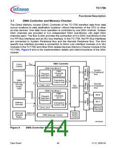
16 independent DMA channels
– 8 DMA channels in each DMA Sub-Block
– Up to 8 selectable request inputs per DMA channel
– 2-level programmable priority of DMA channels within a DMA Sub-Block
– Software and hardware DMA request
– Hardware requests by selected on-chip peripherals and external inputs
Programmable priority of the DMA Sub-Blocks on the bus interfaces
Buffer capability for move actions on the buses (at least 1 move per bus is buffered).
Individually programmable operation modes for each DMA channel
– Single mode: stops and disables DMA channel after a predefined number of DMA
transfers
•
•
•
– Continuous mode: DMA channel remains enabled after a predefined number of
DMA transfers; DMA transaction can be repeated.
– Programmable address modification
•
Full 32-bit addressing capability of each DMA channel
– 4 GByte address range
– Support of circular buffer addressing mode
•
•
•
Programmable data width of DMA transfer/transaction: 8-bit, 16-bit, or 32-bit
Micro Link bus interface support
Register set for each DMA channel
– Source and destination address register
– Channel control and status register
– Transfer count register
•
Flexible interrupt generation (the service request node logic for the MLI channels is
also implemented in the DMA module)
•
•
All buses connected to the DMA module must work at the same frequency.
Read/write requests of the System Bus Side to the Remote Peripherals are bridged
to the Remote Peripheral Bus (only the DMA is master on the RPB)
Memory Checker
The Memory Checker Module (MEMCHK) makes it possible to check the data
consistency of memories. Any SPB bus master may access the memory checker.
Preferable the DMA controller does it as described hereafter. It uses 8-bit, 16-bit, or 32-
bit DMA moves to read from the selected address area and to write the value read in a
memory checker input register. With each write operation to the memory checker input
register, a polynomial checksum calculation is triggered and the result of the calculation
is stored in the memory checker result register.
The memory checker uses the standard Ethernet polynomial, which is given by:
G32 = x32+ x26+ x23+ x22+ x16+ x12+ x11+ x10+ x8+ x7+ x5+ x4+ x2+ x +1
Data Sheet
45
V1.0, 2008-04

 INFINEON [ Infineon ]