TC1796
Electrical Parameters
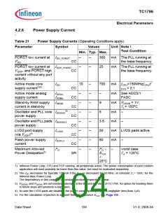
4.2.6
Power Supply Current
???
Table 21
Power Supply Currents (Operating Conditions apply)
Parameter
Symbol
Values
Min. Typ. Max.
Unit Note /
Test Condition
PORST low current at IDD_PORST
–
–
300
mA The PLL running at
the base frequency
VDD
CC
PORST low current at IDDP_PORST
–
–
25
mA The PLL running at
the base frequency
V
DDP, and PORST high
CC
current without any port
activity
Active mode core
IDD
10
–
–
–
–
–
–
–
–
–
700
–
mA
f
CPU=150MHzfCPU/f
supply current1)2)
CC
CC
CC
CC
CC
CC
CC
SR
SYS = 2:1
Active mode analog
supply current
IDDAx;
IDDMx
mA See ADC0/1
FADC
Stand-by RAM supply ISBSB
–
9
mA
mA
mA
VDDSB = 1V,
current in stand-by
Tj = 150oC
3)
Oscillator and PLL core IDDOSC
–
5
–
power supply
Oscillator and PLL pads IDDOSC3
–
3.6
50
80
–
power supply
LVDS port supply
ILVDS
IDDFL3
PD
–
mA LVDS pads active
4)
(via VDDP
)
Flash power supply
current
Maximum Allowed
Power Dissipation5)
–
mA
–
–
–
PD ×
RTJA
<
worst case
TA = 125oC
25oC
1) Infineon Power Loop: CPU and PCP running, all peripherals active. The power consumption of each custom
application will most probably be lower than this value, but must be evaluated separately.
2) The IDD decreases for typically 120 mA if the fCPU is decreased for 50 MHz, at constant TJ = 150C, for the
Infineon Max Power Loop.
The dependency in this range is, at constant junction temperature, linear.
3) VDDOSC and VSSOSC are not bonded externally in the BC and BD steps of TC1796. An option for bonding them
in future steps and products is kept open.
4) In case the LVDS pads are disabled, the power consumption pro pair is negligible (less than 1µA).
5) For the calculation of junction to ambient thermal resistance RTJA, see Page 130.
Data Sheet
104
V1.0, 2008-04

 INFINEON [ Infineon ]