TC1796
Electrical Parameters
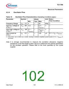
4.2.4
Oscillator Pins
Table 18
Oscillator Pins Characteristics (Operating Conditions apply)
Parameter
Symbol
Min.
fOSC CC 4
Values
Typ. Max.
–
–
Unit Note /
Test Condition
Frequency Range
25
0.3 ×
VDDOSC3
MHz –
Input low voltage at VILX SR -0.2
V
–
XTAL11)
Input high voltage at VIHX SR 0.7 ×
–
–
VDDOSC3
V
–
XTAL11)
VDDOSC3
+ 0.2
Input current at
XTAL1
IIX1 CC –
±25
µA
0 V < VIN < VDDOSC3
1) If the XTAL1 pin is driven by a crystal, reaching a minimum amplitude (peak-to-peak) of 0.3 × VDDOSC3 is
necessary.
Note: It is strongly recommended to measure the oscillation allowance (negative
resistance) in the final target system (layout) to determine the optimal parameters
for the oscillator operation. Please refer to the limits specified by the crystal
supplier.
Data Sheet
102
V1.0, 2008-04

 INFINEON [ Infineon ]