TC1796
Electrical Parameters
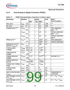
Table 17
FADC Characteristics (Operating Conditions apply) (cont’d)
Parameter
Symbol
Values
Typ. Max.
–
Unit
Note /
Test Condition
Min.
CC –
Conversion time
Converter Clock
Input resistance of
the analog voltage
path (Rn, Rp)
tC
21
CLK of 10-bit conversion
fADC
MHz
kΩ
fADC CC –
–
–
75
200
–
10)
RFAIN
100
CC
Channel Amplifier
Cutoff Frequency
Settling Time of a
Channel Amplifier
after changing ENN
or ENP
fCOFF
tSET
2
–
–
–
5
MHz
–
–
CC
CC –
µsec
1) Calibration of the gain is possible for the gain of 1 and 2, and not possible for the gain of 4 and 8.
2) Calibration should be performed at each power-up. In case of continuous operation, calibration should be
performed minimum once per week.
3) The offset error voltage drifts over the whole temperature range maximum ±3 LSB.
4) Applies when the gain of the channel equals one. For the other gain settings, the offset error increases; it must
be multiplied with the applied gain.
5) Voltage overshoot to 4 V are permissible, provided the pulse duration is less than 100 µs and the cumulated
summary of the pulses does not exceed 1 h.
6) Voltage overshoot to 1.7 V are permissible, provided the pulse duration is less than 100 µs and the cumulated
sum of the pulses does not exceed 1 h.
7) A running conversion may become inexact in case of violating the normal operating conditions (voltage
overshoots).
8) Current peaks of up to 40 mA with a duration of max. 2 ns may occur
9) This value applies in power-down mode.
10) Not subject to production test, verified by design / characterization.
The calibration procedure should run after each power-up, when all power supply
voltages and the reference voltage have stabilized. The offset calibration must run first,
followed by the gain calibration.
Data Sheet
100
V1.0, 2008-04

 INFINEON [ Infineon ]