TC1796
Electrical Parameters
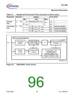
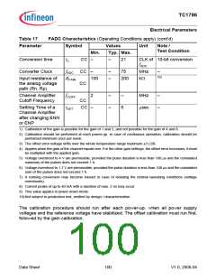
Table 16
Sample and Conversion Time (Operating Conditions apply)
Parameter Symbol
Values
Typ.
Unit Note
Min.
Max.
Sample
time
tS
CC
4 × (CHCONn.STC + 2) × tBC
µs
µs
µs
µs
µs
–
–
8 × tBC
–
–
Conversion tC CC
tS + 40 × tBC + 2 × tDIV
tS + 48 × tBC + 2 × tDIV
tS + 56 × tBC + 2 × tDIV
8-bit conversion
10-bit conversion
12-bit conversion
time
A/D Converter Module
Sample
Programmable
Time tS
fANA
fDIV
fBC
Fractional
Programmable
Counter
fCLC
Clock Divider
1:4
Divider
(1:1) to (1:256)
CON.CTC
CHCONn.STC
fTIMER
Arbiter
Control Unit
(Timer)
Control/Status Logic
Interrupt Logic
(1:20)
External Trigger Logic
External Multiplexer Logic
Request Generation Logic
MCA04657_mod
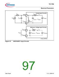
Figure 22
ADC0/ADC1 Clock Circuit
Data Sheet
96
V1.0, 2008-04

 INFINEON [ Infineon ]