TC39x BC/BD-Step
Pin Definition and Functions: LFBGA-516 Package Variant Pin Configuration
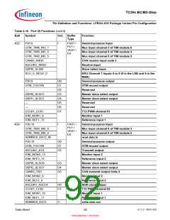
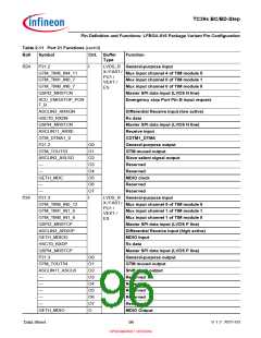
Table 2-11 Port 21 Functions (cont’d)
Ball
Symbol
Ctrl. Buffer
Type
Function
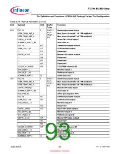
R24
P21.2
I
LVDS_R General-purpose input
X / FAST /
GTM_TIM5_IN4_11
GTM_TIM1_IN0_7
GTM_TIM0_IN0_7
QSPI2_MRSTCN
Mux input channel 4 of TIM module 5
PU1 /
VEXT /
ES
Mux input channel 0 of TIM module 1
Mux input channel 0 of TIM module 0
Master SPI data input (LVDS N line)
Emergency stop Port Pin B input request
SCU_EMGSTOP_POR
T_B
ASCLIN3_ARXGN
HSCT0_RXDN
QSPI4_MRSTCN
ASCLIN11_ARXE
GTM_DTMA1_0
P21.2
Differential Receive input (low active)
Rx data
Master SPI data input (LVDS N line)
Receive input
CDTM1_DTM4
O0
O1
O2
O3
O4
O5
O6
O7
I
General-purpose output
GTM muxed output
Slave select signal output
Reserved
GTM_TOUT53
ASCLIN3_ASLSO
—
—
Reserved
GETH_MDC
—
MDIO clock
Reserved
—
Reserved
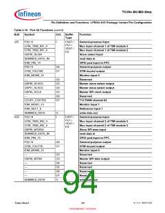
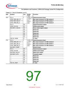
P24
P21.3
LVDS_R General-purpose input
X / FAST /
GTM_TIM5_IN5_12
GTM_TIM1_IN1_6
GTM_TIM0_IN1_6
QSPI2_MRSTCP
ASCLIN3_ARXGP
GETH_MDIOD
HSCT0_RXDP
QSPI4_MRSTCP
P21.3
Mux input channel 5 of TIM module 5
PU1 /
VEXT /
ES
Mux input channel 1 of TIM module 1
Mux input channel 1 of TIM module 0
Master SPI data input (LVDS P line)
Differential Receive input (high active)
MDIO Input
Rx data
Master SPI data input (LVDS P line)
General-purpose output
GTM muxed output
Shift clock output
O0
O1
O2
O3
O4
O5
O6
O7
O
GTM_TOUT54
ASCLIN11_ASCLK
—
Reserved
—
Reserved
—
Reserved
—
Reserved
—
Reserved
GETH_MDIO
MDIO Output
Data Sheet
96
V 1.2, 2021-03
OPEN MARKET VERSION

 INFINEON [ Infineon ]