TC39x BC/BD-Step
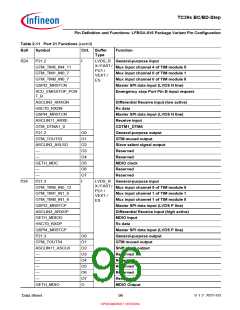
Pin Definition and Functions: LFBGA-516 Package Variant Pin Configuration
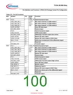
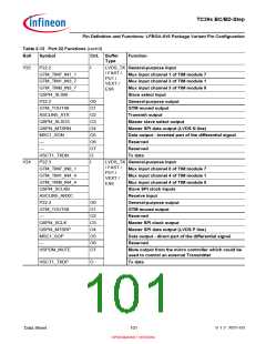
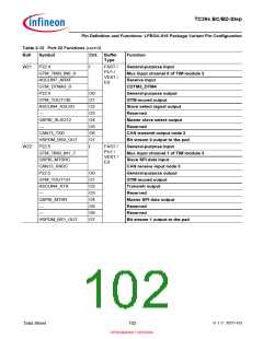
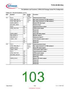
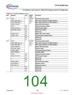
Table 2-12 Port 22 Functions
Ball
Symbol
Ctrl. Buffer
Type
Function
W25
P22.0
I
LVDS_TX General-purpose input
/ FAST /
GTM_TIM7_IN3_1
GTM_TIM1_IN1_7
GTM_TIM0_IN1_7
QSPI4_MTSRB
ASCLIN6_ARXE
P22.0
Mux input channel 3 of TIM module 7
PU1 /
VEXT /
ES6
Mux input channel 1 of TIM module 1
Mux input channel 1 of TIM module 0
Slave SPI data input
Receive input
O0
O1
O2
O3
O4
O5
O6
O7
I
General-purpose output
GTM_TOUT47
ASCLIN3_ATXN
QSPI4_MTSR
QSPI4_SCLKN
MSC1_FCLN
—
GTM muxed output
Differential Transmit output (low active)
Master SPI data output
Master SPI clock output (LVDS N line)
Shift-clock inverted part of the differential signal
Reserved
ASCLIN6_ATX
P22.1
Transmit output
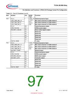
W24
LVDS_TX General-purpose input
/ FAST /
GTM_TIM7_IN2_1
GTM_TIM1_IN0_8
GTM_TIM0_IN0_8
QSPI4_MRSTB
ASCLIN7_ARXE
P22.1
Mux input channel 2 of TIM module 7
PU1 /
VEXT /
ES6
Mux input channel 0 of TIM module 1
Mux input channel 0 of TIM module 0
Master SPI data input
Receive input
O0
O1
O2
O3
General-purpose output
GTM muxed output
GTM_TOUT48
ASCLIN3_ATXP
QSPI4_MRST
IOM_MON2_4
IOM_REF2_4
QSPI4_SCLKP
MSC1_FCLP
—
Differential Transmit output (high active)
Slave SPI data output
Monitor input 2
Reference input 2
O4
O5
O6
O7
Master SPI clock output (LVDS P line)
Shift-clock direct part of the differential signal
Reserved
ASCLIN7_ATX
Transmit output
Data Sheet
100
V 1.2, 2021-03
OPEN MARKET VERSION

 INFINEON [ Infineon ]