TC39x BC/BD-Step
Pin Definition and Functions: LFBGA-516 Package Variant Pin Configuration
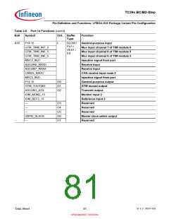
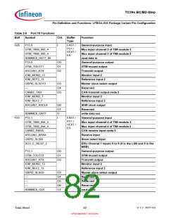
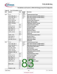
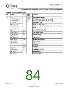
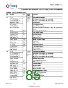
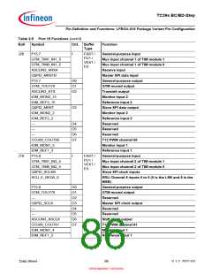
Table 2-9 Port 15 Functions (cont’d)
Ball
Symbol
Ctrl. Buffer
Type
Function
K19
P15.5
I
FAST /
PU1 /
VEXT /
ES
General-purpose input
Mux input channel 0 of TIM module 3
Mux input channel 0 of TIM module 2
Receive input
GTM_TIM3_IN0_4
GTM_TIM2_IN0_4
ASCLIN1_ARXB
I2C0_SDAC
Serial Data Input 2
QSPI2_MTSRA
SCU_E_REQ4_3
Slave SPI data input
ERU Channel 4 inputs 0 to 5 (0 is the LSB and 5 is the
MSB)
P15.5
O0
O1
O2
General-purpose output
GTM muxed output
Transmit output
GTM_TOUT76
ASCLIN1_ATX
IOM_MON2_13
IOM_REF2_13
QSPI2_MTSR
—
Monitor input 2
Reference input 2
O3
O4
O5
O6
O7
Master SPI data output
Reserved
MSC0_EN0
Chip Select
I2C0_SDA
Serial Data Output
CCU60_CC61
IOM_MON1_1
IOM_REF1_5
P15.6
T12 PWM channel 61
Monitor input 1
Reference input 1
F21
I
FAST /
PU1 /
VEXT /
ES
General-purpose input
Mux input channel 2 of TIM module 2
Mux input channel 0 of TIM module 1
Mux input channel 0 of TIM module 0
Slave SPI data input
General-purpose output
GTM muxed output
Transmit output
GTM_TIM2_IN2_14
GTM_TIM1_IN0_6
GTM_TIM0_IN0_6
QSPI2_MTSRB
P15.6
O0
O1
O2
GTM_TOUT77
ASCLIN3_ATX
IOM_MON2_15
IOM_REF2_15
QSPI2_MTSR
QSPI5_SLSO3
QSPI2_SCLK
ASCLIN3_ASCLK
CCU60_CC60
IOM_MON1_2
IOM_REF1_6
Monitor input 2
Reference input 2
O3
O4
O5
O6
O7
Master SPI data output
Master slave select output
Master SPI clock output
Shift clock output
T12 PWM channel 60
Monitor input 1
Reference input 1
Data Sheet
85
V 1.2, 2021-03
OPEN MARKET VERSION

 INFINEON [ Infineon ]