TC39x BC/BD-Step
Electrical SpecificationPeripheral Phase Locked Loop (PER_PLL)
3.17
Peripheral Phase Locked Loop (PER_PLL)
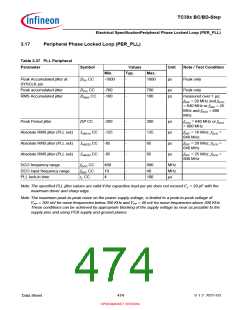
Table 3-37 PLL Peripheral
Parameter
Symbol
Values
Typ.
Unit
Note / Test Condition
Min.
Max.
Peak Accumulated jitter at
SYSCLK pin
D
PP CC
-1000
-
1000
ps
Peak only
Peak accumulated jitter
RMS Accumulated jitter
D
D
PPI CC
-700
-100
-
-
700
100
ps
ps
Peak only
RMS CC
measured over 1 µs;
fREF = 20 MHz and fDCO
= 640 MHz or fREF = 25
MHz and fDCO = 800
MHz
Peak Period jitter
DP CC
-200
-125
-85
-
-
-
-
200
125
85
ps
ps
ps
ps
f
DCO = 640 MHz or fDCO
= 800 MHz
REF = 10 MHz; fDCO
640 MHz
REF = 20 MHz; fDCO
640 MHz
REF = 25 MHz; fDCO
800 MHz
Absolute RMS jitter (PLL out)
Absolute RMS jitter (PLL out)
Absolute RMS jitter (PLL out)
J
J
J
ABS10 CC
ABS20 CC
ABS25 CC
f
=
=
=
f
-85
85
f
DCO frequency range
DCO input frequency range
PLL lock-in time
f
f
DCO CC
REF CC
400
10
4
-
-
-
800
40
MHz
MHz
µs
tL CC
100
Note:The specified PLL jitter values are valid if the capacitive load per pin does not exceed CL = 20 pF with the
maximum driver and sharp edge.
Note:The maximum peak-to-peak noise on the power supply voltage, is limited to a peak-to-peak voltage of
V
PP = 100 mV for noise frequencies below 300 KHz and VPP = 40 mV for noise frequencies above 300 KHz.
These conditions can be achieved by appropriate blocking of the supply voltage as near as possible to the
supply pins and using PCB supply and ground planes.
Data Sheet
474
V 1.2, 2021-03
OPEN MARKET VERSION

 INFINEON [ Infineon ]