TC39x BC/BD-Step
Electrical SpecificationEVR
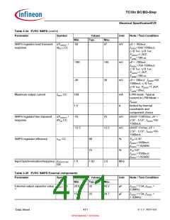
Table 3-35 EVRC SMPS External components (cont’d)
Parameter Symbol
Values
Typ.
Unit
Note / Test Condition
Min.
Max.
50
External output capacitor ESR COUT_ESR
-
-
mOhm f≥0.5MHz ; f≤10MHz
SR
-
-
100
13.5
50
Ohm
µF
f=10Hz
IDDDC=1.5A
External input capacitor value 1) CIN SR
6.5
-
10
External input capacitor ESR
External inductor value
External inductor DCR
C
IN_ESR SR
-
mOhm f≥0.5MHz ; f≤10MHz
-
-
100
6.11
4.29
0.2
Ohm
f=100Hz
L
L
DC SR
3.29
2.31
4.7
3.3
-
f
DCDC=0.8MHz
DCDC=1.82MHz
µH
Ohm
V
f
DC_DCR SR -
LL SR
P + N-channel MOSFET logic
level
V
-
-
2.5
P + N-channel MOSFET drain |VBR_DS| SR +7
-
-
V
V
NMOS - VGS = 0.
PMOS - VGS = 0.
source breakdown voltage
-
-
-7
-
P + N-channel MOSFET drain
source ON-state resistance
R
ON SR
-
-
150
mOhm IDDDC=1.5A; |VGS|=2.5V
; TA=25°C
P + N-channel MOSFET Gate QG SR
-
-
-
8
-
nC
nC
mA
IDDDC=1.5A; NMOS-
|VGS|=5V; 1.5A pulsed
drain current
Charge
-8
IDDDC=1.5A; PMOS-
|VGS|=5V; 1.5A pulsed
drain current
External Inductor Saturation
Current Margin
ΔISAT SR
400
-
The saturation current
of the coil must be
larger than IDDDC
ΔISAT
+
P + N-channel MOSFET Gate
threshold voltage
V
V
GSTH SR
-
-
-
1
-
-
-
V
V
V
NMOS
PMOS
-1
0.8
N-channel MOSFET reverse
diode forward voltage
RDN SR
1) Capacitor min-max range represent typical +-35% tolerance including DC bias effect. The trace resistance from the capacitor
to the supply or ground rail should be limited to 25 mOhm.
Data Sheet
472
V 1.2, 2021-03
OPEN MARKET VERSION

 INFINEON [ Infineon ]