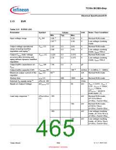
TC39x BC/BD-Step
Electrical SpecificationEVR
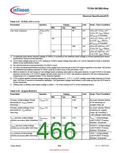
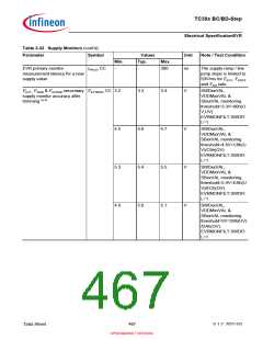
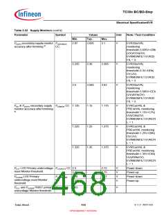
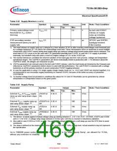
Table 3-32 Supply Monitors (cont’d)
Parameter
Symbol
Values
Typ.
Unit
Note / Test Condition
Min.
Max.
Primary undervoltage reset
threshold for VEXT before
trimming
V
RST5 CC
-
-
3.0
V
by last cold PORST
release on supply
ramp-up including
voltage hysteresis.
EVR secondary monitor
measurement latency for all 6
supply rails
t
MON CC
-
-
3.2
µs
HPOSC and SHPBG
bandgap trimmed.
Filter inactive.
1) The reset release on supply ramp-up is delayed by a time duration 20-40 us after reaching undervoltage reset threshold and
by a voltage hysteresis of 1.5% above the undervoltage reset limit. These mechanisms serve as hysteresis to avoid multiple
consecutive cold PORST events during slow supply ramp-ups owing to voltage drop/current jumps when reset is released. The
reset limit of 2,97V at pin is for the case with 3.3V generated internally from EVR33. In case the 3.3V supply is provided
externally, the bondwire drop will cause a reset at a higher voltage of 3.0V at the VDDP3 pin.
2) The monitor tolerances constitute the inherent variation of the band gap and ADC over process, voltage and temperature
operational ranges. The VxxPRIUV parameters are device individually tested in production with +-1% tolerance about the
VxxPRIUV limits. All voltages are measured on pins.
3) VRSTxx parameters are relevant only for the first cold PORST release. Later the reset levels are trimmed by the Firmware and
reflected as VxxPRIUV parameters before device is used with full performance. The cold PORST is released with a voltage
hysteresis on all the primary monitors to avoid consecutive PORST toggling behavior.
4) In case the application is using 3.3V single supply (Single Supply mode (e), i.e. VEXT and VDDP3 are shorted together), it is
recommended to use secondary supply monitoring on channel VDDP3, because of the better accuracy of parameter
VDDP3MON.
5) To monitor voltage level not provided in conditions the values for OV and UV thresholds can be generated by a linear
interpolation or extrapolation based on the given points.
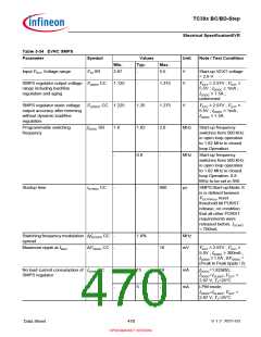
Table 3-33 Supply Ramp
Parameter
Symbol
Values
Typ.
Unit
Note / Test Condition
Min.
Max.
External VEXT & VEVRSB supply dVEXT/dt
8.3E-6
1
100
V/ms
ramp-up and ramp-down slope SR
1) 2) 3)
External VDDP3 supply ramp-up dVDDP3/dt 8.3E-6
1
1
1
100
100
100
V/ms
V/ms
V/ms
and ramp-down slope 1)3)
SR
External VDD supply ramp-up
dVDD/dt
SR
8.3E-6
and ramp-down slope 1)3)
External VDDM supply ramp-up dVDDM/dt 8.3E-6
and ramp-down slope 1)3)
SR
1) The device is robust against residual voltage ramp-up starting between 0 - 2.97 V for VEXT, VEVRSB, VDDP3 and VDDM
and 0-1 V for VDD. A voltage ramp range between 0.5V/min upto 120V/ms is covered in robustness validation.
2) Also valid in case EVR33 or EVRC is used. The generated voltage itself follows a soft ramp-up over the tSTR time to avoid
overshoots.
3) The slope is defined as the maximal tangential slope between 0% to 100% voltage level. Actual waveform may not represent
the specification.
Up to 1000000 power-cycles, matching the limits defined in the table ’Supply Ramp’, are allowed for TC39x,
without any restriction to reliability.
Data Sheet
469
V 1.2, 2021-03
OPEN MARKET VERSION

 INFINEON [ Infineon ]