TC39x BC/BD-Step
Electrical SpecificationPin Reliability in Overload
3.3
Pin Reliability in Overload
When receiving signals from higher voltage devices, low-voltage devices experience overload currents and
voltages that go beyond their own IO power supplies specification.
The following table defines overload conditions that will not cause any negative reliability impact if all the following
conditions are met:
•
allowed time interval (defined in Note column) for overload condition is not exceeded. If no time limit is defined
the allowed time includes both ‘Operation Lifetime hours’ and ‘Inactive Lifetime hours’. The number of hours
in Table 3-77 and Table 3-78 are examples only and the applicable numbers are defined by the customer
profiles accepted by Infineon.
•
Operating Conditions are met for
–
–
pad supply levels
temperature
If a pin current is out of the Operating Conditions but within the overload parameters, then the parameters
functionality of this pin as stated in the Operating Conditions can no longer be guaranteed. Operation is still
possible in most cases but with relaxed parameters.
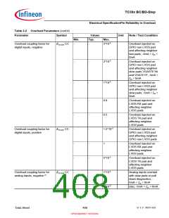
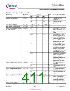
Table 3-2 Overload Parameters
Parameter
Symbol
Values
Typ.
Unit
Note / Test Condition
Min.
-5
-15 1)
Max.
5
15 1)
Input current on any digital pin IIN
during overload condition
-
-
mA
mA
except LVDS pins
except LVDS pins;
limited to max. 20
pulses with 1ms pulse
length
Input current on LVDS pin
during overload condition
IINLVDS
-3
-
3
mA
Input current on analog input pin IINANA
during overload condition
-3
-5
-
-
3
5
mA
mA
limited to 60h over
lifetime
Absolute sum of all analog input IINSA
currents for analog inputs during
overload condition
-20
-
-
20
mA
mA
Absolute maximum sum of all
input circuit currents during
overload condition (digital and
analog combined)
ΣIINS
-100
100
Signal voltage over/undershoot VOUS
at GPIOs
V
SS - 2
-
VEXT/FLEX
+ 2
V
limited to 60h over
lifetime; Valid for non
LVDS and analoge
pads
Sum of all inactive device pin
currents
IIDS
-100
-
-
-
100
2.5
5
mA
mA
mA
Static pin output current
I
OUT CC
-
-
100% duty cycle;
output driver = medium
100% duty cycle;
output driver = strong
Data Sheet
407
V 1.2, 2021-03
OPEN MARKET VERSION

 INFINEON [ Infineon ]