TC39x BC/BD-Step
Electrical SpecificationAbsolute Maximum Ratings
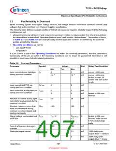
3.2
Absolute Maximum Ratings
Stresses above the values listed under “Absolute Maximum Ratings” may cause permanent damage to the device.
This is a stress rating only and functional operation of the device at these or any other conditions above those
indicated in the Operational Conditions of this specification is not implied. Exposure to absolute maximum rating
conditions may affect device reliability.
Table 3-1 Absolute Maximum Ratings
Parameter
Symbol
Values
Typ.
Unit
Note / Test Condition
Min.
Max.
150
Storage Temperature
T
ST SR
-65
-
-
-
-
°C
V
upto 65h @ TJ = 150°C
upto 2.8h
Voltage at VDD power supply
pins with respect to VSS
V
DD SR
-
-
-
1.65
1.45
4.43
1) 2)
V
upto 72h
Voltage at VDDP3 power supply
pins with respect to VSS
V
DDP3 SR
V
Voltage at VDDM, VEXT, VFLEX and VDDM SR
EVRSB power supply pins with
respect to VSS
-
-
-
-
6.75
5.6
V
V
upto 2.8h
upto 72h
V
Voltage on all analog and class VIN SR
-0.7
-
6.75
V
S input pins with respect to VSS
3)
Voltage on all other input pins
with respect to VSS
VIN SR
-0.7
-10
-
-
-
6.75
10
V
3)
Input current on any pin during IIN SR
mA
mA
4) 5)
overload condition
Absolute maximum sum of all
input circuit currents during
overload condition. 4)
ΣIIN SR
-100
100
1) Valid for cumulated for up to 2.8h and pulse forms followed a power supply switch on phase, where the rise
and fall times are related to the system capacities and coils.
2) Due to EVRC output voltage oscillation during switch off phase VDD can drop down to -0.72V. For VDD an input level down to
-0.72V during switch off phase will not cause any damage or reliability problem.
3) Voltages below VINmin have no Impact to the device reliability as Long as the times and currents defined in section Pin Reliability
in Overload for the affected pad(s) are not violated.
4) This parameter is an Absolute Maximum Rating. Exposure to Absolute Maximum Ratings for extended periods of time may
damage the device.
5) The specified min. and max. values represent the current limits, which have to be maintained, in case of a short circuit condition
on the output of any Fast, RFast, Slow and Class S pad, not being used during operation.
This covers also output currents due to switching in operation for CL=200pF.
Data Sheet
406
V 1.2, 2021-03
OPEN MARKET VERSION

 INFINEON [ Infineon ]