TC39x BC/BD-Step
Pin Definition and Functions: LFBGA-292 ADAS Package Variant Pin
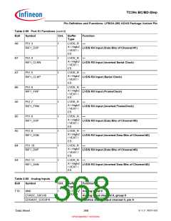
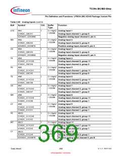
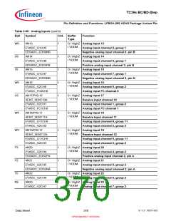
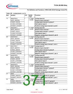
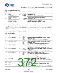
Table 2-60 Analog Inputs (cont’d)
Ball
Symbol
Ctrl. Buffer
Type
Function
U2
AN46
I
I
D / HighZ Analog Input 46
/ VDDM
EVADC_G8CH14
EDSADC_EDS1PD
AN47
Analog input channel 14, group 8
Positive analog input channel 1, pin D
D / HighZ Analog Input 47
P4
/ VDDM
EVADC_G8CH15
EDSADC_EDS1ND
Analog input channel 15, group 8
Negative analog input channel 1, pin D
Note: Port Pins P32.0 and P32.1 are bidirectional pads and are having the following two functionalities
implemented:
5. In case the pins are used as standard GPIOs the functions defined in the pin configuration tables of P32.0 and
P32.1 are available.
6. In case the pins are used as pre-drivers for external MOSFETs (internal DCDC usecase) P32.0 and P32.1 act
as analog IOs named VGATE1N and VGATE1P.
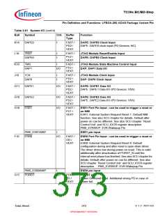
Table 2-61 System I/O
Ball
Symbol
Ctrl. Buffer
Type
Function
L7
AGBTCLKN (VSS)
I
AGBT_C Input PAD (negative pole) for the external 100 MHz
LK /
differential clock.
VEXT
AGBT Input; (TC3xx devices without AGBT: VSS)
K7
AGBTCLKP (VSS)
AGBTTXN (VSS)
AGBTTXP (VSS)
AGBTERR (VSS)
I
AGBT_C Input PAD (positive pole) for the external 100 MHz
LK /
differential clock.
VEXT
AGBT Input; (TC3xx devices without AGBT: VSS)
P10
P11
L14
O
O
I
AGBT_T Off-chip driver output PAD of the 2.5Gbps transmitter,
X / VEXT negative pole
AGBT Output; (TC3xx devices without AGBT: VSS)
AGBT_T Off-chip driver output PAD of the 2.5Gbps transmitter,
X / VEXT positive pole
AGBT Output; (TC3xx devices without AGBT: VSS)
FAST /
PD /
Input PAD for CRC error from FPGA.
AGBT Input; (TC3xx devices without AGBT: VSS)
VEXT
W17
Y17
VGATE1P
VGATE1N
O
O
—
DCDC P ch. MOSFET gate driver output
P32.1 / External Pass Device gate control for EVRC
—
DCDC N ch. MOSFET gate driver output
P32.0 / SMPS mode: analog output. External Pass Device
gate control for EVRC
M20
M19
XTAL1
XTAL2
I
XTAL /
VEXT
XTAL pad1
XTAL1. Main Oscillator/PLL/Clock Generator Input.
O
XTAL /
VEXT
XTAL pad2
XTAL2. Main Oscillator/PLL/Clock Generator OUTPUT
Data Sheet
372
V 1.2, 2021-03
OPEN MARKET VERSION

 INFINEON [ Infineon ]