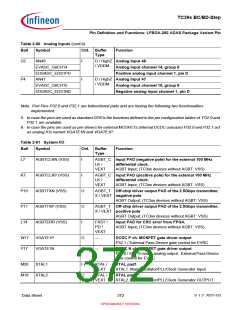
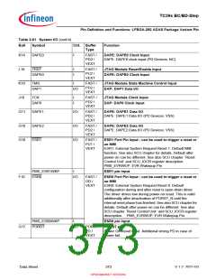
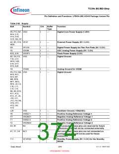
TC39x BC/BD-Step
Pin Definition and Functions: LFBGA-292 ADAS Package Variant Pin
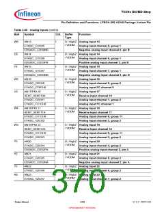
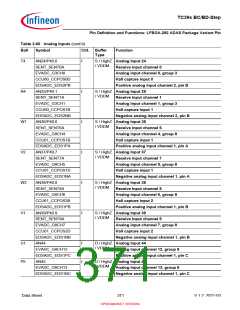
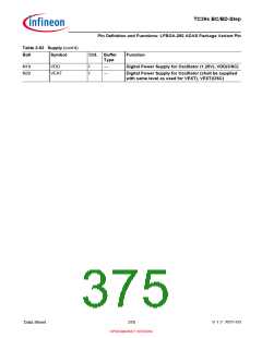
Table 2-60 Analog Inputs (cont’d)
Ball
Symbol
Ctrl. Buffer
Type
Function
T4
AN24/P40.0
I
I
I
I
I
I
S / HighZ Analog Input 24
/ VDDM
SENT_SENT0A
EVADC_G3CH0
CCU60_CCPOS0D
EDSADC_EDS2PB
AN25/P40.1
Receive input channel 0
Analog input channel 0, group 3
Hall capture input 0
Positive analog input channel 2, pin B
R4
W1
V2
W2
V1
S / HighZ Analog Input 25
/ VDDM
SENT_SENT1A
EVADC_G3CH1
CCU60_CCPOS1B
EDSADC_EDS2NB
AN36/P40.6
Receive input channel 1
Analog input channel 1, group 3
Hall capture input 1
Negative analog input channel 2, pin B
S / HighZ Analog Input 36
/ VDDM
SENT_SENT6A
EVADC_G8CH4
CCU61_CCPOS1B
EDSADC_EDS1PA
AN37/P40.7
Receive input channel 6
Analog input channel 4, group 8
Hall capture input 1
Positive analog input channel 1, pin A
S / HighZ Analog Input 37
/ VDDM
SENT_SENT7A
EVADC_G8CH5
CCU61_CCPOS1D
EDSADC_EDS1NA
AN38/P40.8
Receive input channel 7
Analog input channel 5, group 8
Hall capture input 1
Negative analog input channel 1, pin A
S / HighZ Analog Input 38
/ VDDM
SENT_SENT8A
EVADC_G8CH6
CCU61_CCPOS2B
EDSADC_EDS1PB
AN39/P40.9
Receive input channel 8
Analog input channel 6, group 8
Hall capture input 2
Positive analog input channel 1, pin B
S / HighZ Analog Input 39
/ VDDM
SENT_SENT9A
EVADC_G8CH7
CCU61_CCPOS2D
EDSADC_EDS1NB
AN44
Receive input channel 9
Analog input channel 7, group 8
Hall capture input 2
Negative analog input channel 1, pin B
U1
P5
I
I
D / HighZ Analog Input 44
/ VDDM
EVADC_G8CH12
EDSADC_EDS1PC
AN45
Analog input channel 12, group 8
Positive analog input channel 1, pin C
D / HighZ Analog Input 45
/ VDDM
EVADC_G8CH13
EDSADC_EDS1NC
Analog input channel 13, group 8
Negative analog input channel 1, pin C
Data Sheet
371
V 1.2, 2021-03
OPEN MARKET VERSION

 INFINEON [ Infineon ]