TC39x BC/BD-Step
Pin Definition and Functions: LFBGA-516 Package Variant Pin Configuration
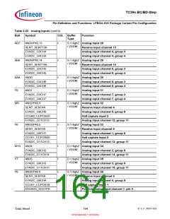
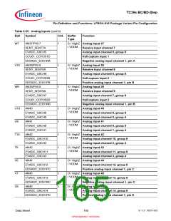
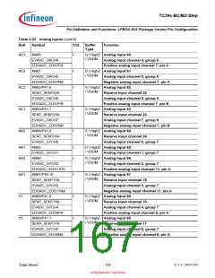
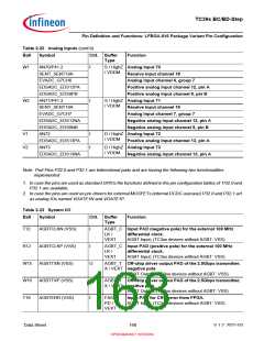
Table 2-22 Analog Inputs (cont’d)
Ball
Symbol
Ctrl. Buffer
Type
Function
W1
AN70/P41.2
I
S / HighZ Analog Input 70
/ VDDM
SENT_SENT18A
EVADC_G7CH6
EDSADC_EDS12PA
EDSADC_EDS9PB
AN71/P41.3
Receive input channel 18
Analog input channel 6, group 7
Positive analog input channel 12, pin A
Positive analog input channel 9, pin B
W2
I
S / HighZ Analog Input 71
/ VDDM
SENT_SENT19A
EVADC_G7CH7
EDSADC_EDS12NA
EDSADC_EDS9NB
AN72
Receive input channel 19
Analog input channel 7, group 7
Negative analog input channel 12, pin A
Negative analog input channel 9, pin B
V1
V2
I
I
D / HighZ Analog Input 72
/ VDDM
EDSADC_EDS13PA
AN73
Positive analog input channel 13, pin A
D / HighZ Analog Input 73
/ VDDM
EDSADC_EDS13NA
Negative analog input channel 13, pin A
Note: Port Pins P32.0 and P32.1 are bidirectional pads and are having the following two functionalities
implemented:
1. In case the pins are used as standard GPIOs the functions defined in the pin configuration tables of P32.0 and
P32.1 are available.
2. In case the pins are used as pre-drivers for external MOSFETs (internal DCDC usecase) P32.0 and P32.1 act
as analog IOs named VGATE1N and VGATE1P.
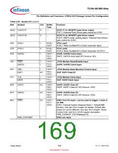
Table 2-23 System I/O
Ball
Symbol
Ctrl. Buffer
Type
Function
T12
AGBTCLKN (VSS)
I
AGBT_C Input PAD (negative pole) for the external 100 MHz
LK /
differential clock.
VEXT
AGBT Input; (TC3xx devices without AGBT: VSS)
R12
W15
W16
T19
AGBTCLKP (VSS)
AGBTTXN (VSS)
AGBTTXP (VSS)
AGBTERR (VSS)
I
AGBT_C Input PAD (positive pole) for the external 100 MHz
LK /
differential clock.
VEXT
AGBT Input; (TC3xx devices without AGBT: VSS)
O
O
I
AGBT_T Off-chip driver output PAD of the 2.5Gbps transmitter,
X / VEXT negative pole
AGBT Output; (TC3xx devices without AGBT: VSS)
AGBT_T Off-chip driver output PAD of the 2.5Gbps transmitter,
X / VEXT positive pole
AGBT Output; (TC3xx devices without AGBT: VSS)
FAST /
PD /
Input PAD for CRC error from FPGA.
AGBT Input; (TC3xx devices without AGBT: VSS)
VEXT
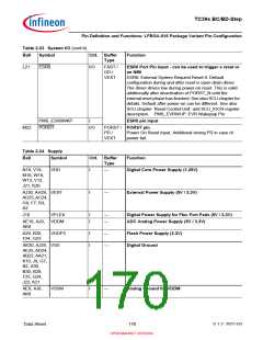
Data Sheet
168
V 1.2, 2021-03
OPEN MARKET VERSION

 INFINEON [ Infineon ]