TC39x BC/BD-Step
Pin Definition and Functions: LFBGA-516 Package Variant Pin Configuration
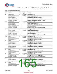
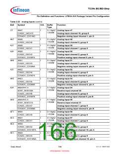
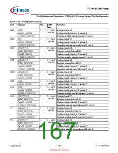
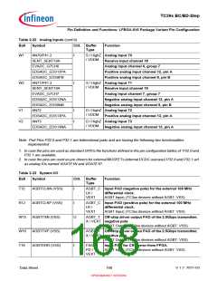
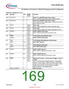
Table 2-23 System I/O (cont’d)
Ball Symbol
Ctrl. Buffer
Type
Function
AD22 VGATE1P
AE22 VGATE1N
O
—
DCDC P ch. MOSFET gate driver output
P32.1 / External Pass Device gate control for EVRC
O
—
DCDC N ch. MOSFET gate driver output
P32.0 / SMPS mode: analog output. External Pass Device
gate control for EVRC
U25
U24
R19
XTAL1
XTAL2
DAPE0
I
XTAL /
VEXT
XTAL pad1
XTAL1. Main Oscillator/PLL/Clock Generator Input.
O
I
XTAL /
VEXT
XTAL pad2
XTAL2. Main Oscillator/PLL/Clock Generator OUTPUT
FAST /
PD2 /
VEXT
DAPE: DAPE0 Clock Input
DAPE: DAPE0 clock input (PD Devices: NC)
T24
R21
P21
M16
M15
M21
TRST
I
I
FAST /
PU2 /
VEXT
JTAG Module Reset/Enable Input
DAPE: DAPE0 Clock Input
DAPE0
TMS
I
FAST /
PD2 /
VEXT
JTAG Module State Machine Control Input
DAP: DAP1 Data I/O
DAP1
I/O
TCK
I
I
FAST /
PD2 /
VEXT
JTAG Module Clock Input
DAP: DAP0 Clock Input
DAP0
DAPE1
DAPE2
ESR1
I/O
I/O
I/O
FAST /
PD2 /
VEXT
DAPE: DAPE1 Data I/O
DAPE: DAPE1 Data I/O (PD Devices: VSS)
FAST /
PD2 /
VEXT
DAPE: DAPE2 Data I/O
DAPE: DAPE2 Data I/O (PD Devices: VSS)
FAST /
PU1 /
VEXT
ESR1 Port Pin input - can be used to trigger a reset or
an NMI
ESR1: External System Request Reset 1. Default NMI
function. See also SCU chapter for details. Default after
power-on can be different. See also SCU chapter ´Reset
Control Unit´ and SCU_IOCR register description.
PMS_EVRWUP: EVR Wakepup Pin
PMS_ESR1WKP
I
ESR1 pin input
Data Sheet
169
V 1.2, 2021-03
OPEN MARKET VERSION

 INFINEON [ Infineon ]