TC39x BC/BD-Step
Pin Definition and Functions: LFBGA-516 Package Variant Pin Configuration
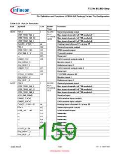
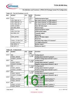
Table 2-21 Port 34 Functions (cont’d)
Ball
Symbol
Ctrl. Buffer
Type
Function
AB18 P34.5
GTM_TIM5_IN7_9
I
FAST /
PU1 /
VEVRSB
/ ES
General-purpose input
Mux input channel 7 of TIM module 5
Mux input channel 7 of TIM module 4
Mux input channel 7 of TIM module 2
Slave SPI data input
GTM_TIM4_IN7_12
GTM_TIM2_IN7_9
QSPI2_MTSRD
ASCLIN8_ARXE
P34.5
Receive input
O0
O1
O2
O3
O4
O5
O6
O7
General-purpose output
GTM muxed output
GTM_TOUT150
ASCLIN8_ATX
—
Transmit output
Reserved
QSPI2_MTSR
—
Master SPI data output
Reserved
EVADC_FC7BFLOUT
CCU60_COUT61
IOM_MON1_4
IOM_REF1_2
Boundary flag output, FC channel 7
T12 PWM channel 61
Monitor input 1
Reference input 1
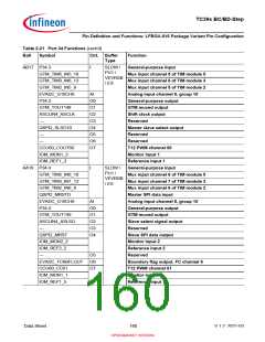
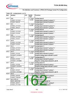
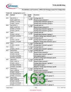
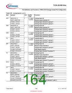
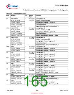
Table 2-22 Analog Inputs
Ball
Symbol
Ctrl. Buffer
Type
Function
AA15 AN0
EVADC_G0CH0
EDSADC_EDS3PA
AB15 AN1
I
I
I
I
I
I
D / HighZ Analog Input 0
/ VDDM
Analog input channel 0, group 0
Positive analog input channel 3, pin A
D / HighZ Analog Input 1
/ VDDM
EVADC_G0CH1
Analog input channel 1, group 0
Negative analog input channel 3, pin A
D / HighZ Analog Input 2
EDSADC_EDS3NA
AD14 AN2
/ VDDM
EVADC_G0CH2
Analog input channel 2, group 0
EDSADC_EDS0PA
Positive analog input channel 0, pin A
AB14 AN3
D / HighZ Analog Input 3
/ VDDM
EVADC_G0CH3
Analog input channel 3, group 0
Negative analog input channel 0, pin A
D / HighZ Analog Input 4
EDSADC_EDS0NA
AA14 AN4
/ VDDM
EVADC_G11CH0
EVADC_G0CH4
Analog input channel 0, group 11
Analog input channel 4, group 0
AE14 AN5
D / HighZ Analog Input 5
/ VDDM
EVADC_G11CH1
EVADC_G0CH5
Analog input channel 1, group 11
Analog input channel 5, group 0
Data Sheet
161
V 1.2, 2021-03
OPEN MARKET VERSION

 INFINEON [ Infineon ]