C167CR
C167SR
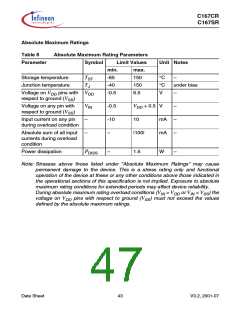
Absolute Maximum Ratings
Table 8
Absolute Maximum Rating Parameters
Parameter
Symbol
Limit Values
Unit Notes
min.
max.
150
150
6.5
Storage temperature
Junction temperature
TST
TJ
-65
-40
-0.5
°C
°C
V
–
under bias
Voltage on VDD pins with VDD
respect to ground (VSS)
–
Voltage on any pin with
respect to ground (VSS)
VIN
-0.5
-10
–
V
DD + 0.5 V
–
–
–
Input current on any pin
during overload condition
–
10
mA
mA
Absolute sum of all input
currents during overload
condition
–
|100|
Power dissipation
PDISS
–
1.5
W
–
Note: Stresses above those listed under “Absolute Maximum Ratings” may cause
permanent damage to the device. This is a stress rating only and functional
operation of the device at these or any other conditions above those indicated in
the operational sections of this specification is not implied. Exposure to absolute
maximum rating conditions for extended periods may affect device reliability.
During absolute maximum rating overload conditions (VIN > VDD or VIN < VSS) the
voltage on VDD pins with respect to ground (VSS) must not exceed the values
defined by the absolute maximum ratings.
Data Sheet
43
V3.2, 2001-07

 INFINEON [ Infineon ]