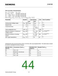
C167CR
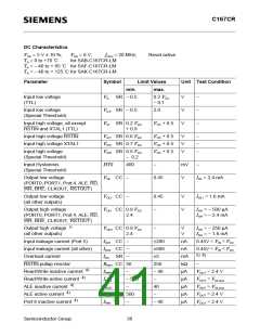
Parameter
Symbol
Limit Values
max.
Unit Test Condition
min.
4)
3)
Port 6 active current
IP6L
– 500
–
–
µA
µA
µA
µA
pF
VOUT = VOL1max
4)
2)
PORT0 configuration current
IP0H
– 10
–
VIN = VIHmin
3)
IP0L
– 100
VIN = VILmax
XTAL1 input current
IIL
CC –
± 20
10
0 V < VIN < VCC
5)
Pin capacitance
CIO CC –
f = 1 MHz
TA = 25 °C
(digital inputs/outputs)
Power supply current
ICC
IID
–
–
–
20 +
5 × fCPU
mA
mA
µA
RSTIN = VIL2
6)
fCPU in [MHz]
Idle mode supply current
20 +
2 × fCPU
RSTIN = VIH1
fCPU in [MHz]
6)
7)
Power-down mode supply current IPD
100
VCC = 5.5 V
Notes
1)
This specification is not valid for outputs which are switched to open drain mode. In this case the respective
output will float and the voltage results from the external circuitry.
2)
3)
4)
The maximum current may be drawn while the respective signal line remains inactive.
The minimum current must be drawn in order to drive the respective signal line active.
This specification is only valid during Reset, or during Hold- or Adapt-mode. Port 6 pins are only affected, if
they are used for CS output and the open drain function is not enabled.
5)
6)
Not 100 % tested, guaranteed by design characterization.
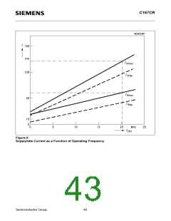
The supply current is a function of the operating frequency. This dependency is illustrated in the figure below.
These parameters are tested at VCCmax and 20 MHz CPU clock with all outputs disconnected and all inputs at
VIL or VIH.
7)
8)
This parameter is tested including leakage currents. All inputs (including pins configured as inputs) at 0 V to
0.1 V or at VCC – 0.1 V to VCC, VREF = 0 V, all outputs (including pins configured as outputs) disconnected.
Overload conditions occur if the standard operatings conditions are exceeded, i.e. the voltage on any pin
exceeds the specified range (i.e. VOV > VCC + 0.5 V or VOV < VSS – 0.5V). The absolute sum of input overload
currents on all port pins may not exceed 50 mA.
Semiconductor Group
39

 INFINEON [ Infineon ]