C167CR
Pin Definitions and Functions (cont’d)
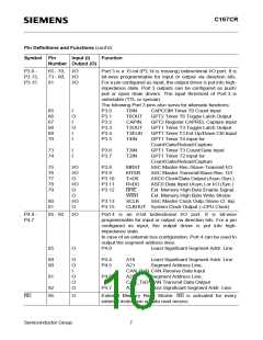
Symbol Pin
Input (I)
Function
Number Output (O)
WR/
WRL
96 O
External Memory Write Strobe. In WR-mode this pin is
activated for every external data write access. In WRL-mode
this pin is activated for low byte data write accesses on a 16-
bit bus, and for every data write access on an 8-bit bus. See
WRCFG in register SYSCON for mode selection.
READY 97
I
Ready Input. When the Ready function is enabled, a high
level at this pin during an external memory access will force
the insertion of memory cycle time waitstates until the pin
returns to a low level.
ALE
EA
98
99
O
I
Address Latch Enable Output. Can be used for latching the
address into external memory or an address latch in the
multiplexed bus modes.
External Access Enable pin. A low level at this pin during and
after Reset forces the C167CR to begin instruction execution
out of external memory. A high level forces execution out of
the internal ROM. ROMless versions must have this pin tied
to ‘0’.
PORT0:
P0L.0 -
P0L.7,
P0H.0 - 108,
P0H.7 111-117
I/O
PORT0 consists of the two 8-bit bidirectional I/O ports P0L
and P0H. It is bit-wise programmable for input or output via
direction bits. For a pin configured as input, the output driver
is put into high-impedance state.
In case of an external bus configuration, PORT0 serves as
the address (A) and address/data (AD) bus in multiplexed bus
modes and as the data (D) bus in demultiplexed bus modes.
Demultiplexed bus modes:
100 -
107
Data Path Width:
P0L.0 - P0L.7:
P0H.0 - P0H.7:
8-bit
D0 - D7
I/O
16-bit
D0 - D7
D8 - D15
Multiplexed bus modes:
Data Path Width:
P0L.0 - P0L.7:
P0H.0 - P0H.7:
8-bit
AD0 - AD7
A8 - A15
16-bit
AD0 - AD7
AD8 - AD15
Semiconductor Group
8

 INFINEON [ Infineon ]