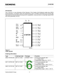
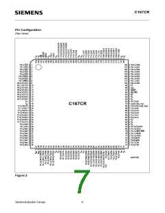
C167CR
Pin Definitions and Functions (cont’d)
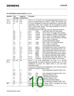
Symbol Pin Input (I) Function
Number Output (O)
P3.0 -
P3.13,
P3.15
65 - 70, I/O
73 - 80, I/O
Port 3 is a 15-bit (P3.14 is missing) bidirectional I/O port. It is
bit-wise programmable for input or output via direction bits.
For a pin configured as input, the output driver is put into high-
impedance state. Port 3 outputs can be configured as push/
pull or open drain drivers. The input threshold of Port 3 is
selectable (TTL or special).
81
I/O
The following Port 3 pins also serve for alternate functions:
65
66
67
68
69
70
I
O
I
O
I
I
P3.0
P3.1
P3.2
P3.3
P3.4
P3.5
T0IN
CAPCOM Timer T0 Count Input
GPT2 Timer T6 Toggle Latch Output
GPT2 Register CAPREL Capture Input
GPT1 Timer T3 Toggle Latch Output
GPT1 Timer T3 Ext.Up/Down Ctrl.Input
GPT1 Timer T4 Input for
T6OUT
CAPIN
T3OUT
T3EUD
T4IN
Count/Gate/Reload/Capture
73
74
I
I
P3.6
P3.7
T3IN
T2IN
GPT1 Timer T3 Count/Gate Input
GPT1 Timer T2 Input for
Count/Gate/Reload/Capture
75
76
77
78
79
I/O
I/O
O
I/O
O
O
I/O
O
P3.8
P3.9
P3.10
P3.11
P3.12
MRST
MTSR
T×D0
R×D0
BHE
SSC Master-Rec./Slave-Transmit I/O
SSC Master-Transmit/Slave-Rec. O/I
ASC0 Clock/Data Output (Asyn./Syn.)
ASC0 Data Input (Asyn.) or I/O (Syn.)
Ext. Memory High Byte Enable Signal,
Ext. Memory High Byte Write Strobe
SSC Master Clock Outp./Slave Cl. Inp.
WRH
SCLK
80
81
P3.13
P3.15
CLKOUT System Clock Output (=CPU Clock)
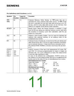
P4.0 -
P4.7
85 - 92
I/O
Port 4 is an 8-bit bidirectional I/O port. It is bit-wise
programmable for input or output via direction bits. For a pin
configured as input, the output driver is put into high-
impedance state.
In case of an external bus configuration, Port 4 can be used to
output the segment address lines:
85
...
89
90
O
...
O
O
I
O
O
O
P4.0
...
P4.4
P4.5
Least Significant Segment Addr. Line
...
Least Significant Segment Addr. Line
Segment Address Line,
...
A16
A21
CAN_RxD CAN Receive Data Input
A22 Segment Address Line,
CAN_TxD CAN Transmit Data Output
A23 Most Significant Segment Addr. Line
91
P4.6
P4.7
92
95
RD
O
External Memory Read Strobe. RD is activated for every
external instruction or data read access.
Semiconductor Group
7

 INFINEON [ Infineon ]