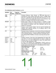
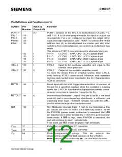
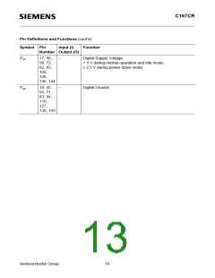
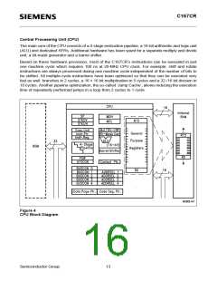
C167CR
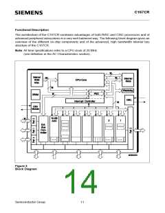
Memory Organization
The memory space of the C167CR is configured in a Von Neumann architecture which means that
code memory, data memory, registers and I/O ports are organized within the same linear address
space which includes 16 MBytes. The entire memory space can be accessed bytewise or wordwise.
Particular portions of the on-chip memory have additionally been made directly bitaddressable.
The C167CR is prepared to incorporate on-chip mask-programmable ROM or Flash Memory for
code or constant data. Currently no ROM is integrated.
2 KBytes of on-chip Internal RAM are provided as a storage for user defined variables, for the
system stack, general purpose register banks and even for code. A register bank can consist of up
to 16 wordwide (R0 to R15) and/or bytewide (RL0, RH0, …, RL7, RH7) so-called General Purpose
Registers (GPRs).
1024 bytes (2 × 512 bytes) of the address space are reserved for the Special Function Register
areas (SFR space and ESFR space). SFRs are wordwide registers which are used for controlling
and monitoring functions of the different on-chip units. Unused SFR addresses are reserved for
future members of the C16x family.
2 KBytes of on-chip Extension RAM (XRAM) are provided to store user data, user stacks or code.
The XRAM is accessed like external memory and therefore cannot be used for the system stack or
for register banks and is not bitadressable. The XRAM allows 16-bit accesses with maximum
speed.
In order to meet the needs of designs where more memory is required than is provided on chip, up
to 16 MBytes of external RAM and/or ROM can be connected to the microcontroller.
External Bus Controller
All of the external memory accesses are performed by a particular on-chip External Bus Controller
(EBC). It can be programmed either to Single Chip Mode when no external memory is required, or
to one of four different external memory access modes, which are as follows:
– 16-/18-/20-/24-bit Addresses, 16-bit Data, Demultiplexed
– 16-/18-/20-/24-bit Addresses, 16-bit Data, Multiplexed
– 16-/18-/20-/24-bit Addresses, 8-bit Data, Multiplexed
– 16-/18-/20-/24-bit Addresses, 8-bit Data, Demultiplexed
In the demultiplexed bus modes, addresses are output on PORT1 and data is input/output on
PORT0. In the multiplexed bus modes both addresses and data use PORT0 for input/output.
Important timing characteristics of the external bus interface (Memory Cycle Time, Memory Tri-
State Time, Length of ALE and Read Write Delay) have been made programmable to allow the user
the adaption of a wide range of different types of memories. In addition, different address ranges
may be accessed with different bus characteristics. Up to 5 external CS signals can be generated
in order to save external glue logic. Access to very slow memories is supported via a particular
‘Ready’ function. A HOLD/HLDA protocol is available for bus arbitration.
For applications which require less than 16 MBytes of external memory space, this address space
can be restricted to 1 MByte, 256 KByte or to 64 KByte. In this case Port 4 outputs four, two or no
address lines at all. It outputs all 8 address lines, if an address space of 16 MBytes is used.
Semiconductor Group
12

 INFINEON [ Infineon ]