SAE 81C90/91
07Feb95@09:05h Intermediate Version
Device Control and Registers
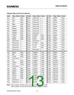
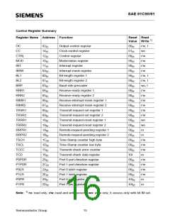
The operation of the SAE 81C90/91 is controlled via a number of registers. These registers allow
initialization and function control, provide status information and configure the message objects.
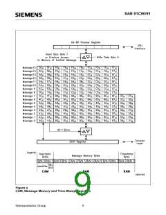
The upper part of the address space provides access to the data buffers of the message objects.
The data buffers are ordered sequentially as shown in the table below.
The register map on the next page summarizes the other registers (i.e. except the data registers)
ordered by their address, while the following pages describe these registers in more detail from a
functional point of view.
Note: Locations marked “Reserved” in the register map must not be written in initialization mode.
This also applies to locations 60 through 7F .
H
H
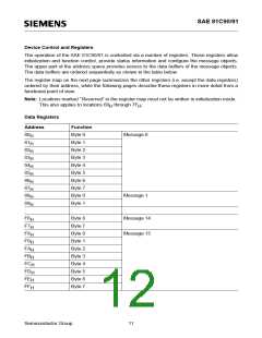
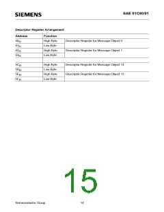
Data Registers
Address
Function
Byte 0
Byte 1
Byte 2
Byte 3
Byte 4
Byte 5
Byte 6
Byte 7
Byte 0
Byte 1
:
80
H
Message 0
81
H
82
H
83
H
84
H
85
H
86
H
87
H
88
H
Message 1
89
H
:
:
F6
H
Byte 6
Byte 7
Byte 0
Byte 1
Byte 2
Byte 3
Byte 4
Byte 5
Byte 6
Byte 7
Message 14
F7
H
F8
H
Message 15
F9
H
FA
H
FB
H
FC
H
FD
H
FE
H
FF
H
Semiconductor Group
11

 INFINEON [ Infineon ]