SAE 81C90/91
07Feb95@09:05h Intermediate Version
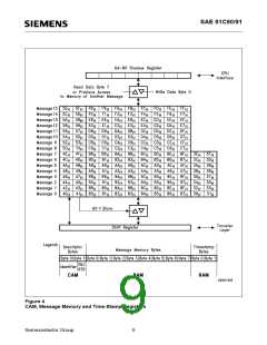
Time Stamp
It is impossible to determine from the received data in the message memory when they were
received. So the host controller is unable to derive any information about the actuality or the
repetition rate of the data.
To enable an indication of the time of reception for at least some of the messages, a 16-bit timer is
implemented on the SAE 81C90/91. The content of this gets written into the time-stamp registers of
the particular message when it is received (for the messages 0 through 7). There are two time-
stamp bytes for each of the messages 0 through 7, and these hold the value of the 16-bit timer.
The actuality of a message is determined by subtracting the old time-stamp of a message, stored in
the host controller, from the new one, with respect to the timer overflow bit.
Overflow of the timer can be detected by bit TSOV in the CTRL register. This bit does not trigger an
interrupt and has to be reset by the host controller. Depending on the setting of bitfield TSP in
register CTRL, the counter is fed with 1/32, 1/64, 1/128 or 1/256 of the bus clock. The momentary
timer status can be read and set at any time. The timer starts at 0 after a reset and cannot be
stopped.
I/O-Ports
There are two parallel I/O ports in the SAE 81C90, each with eight pins. These ports are configured
pin by pin as input or output, depending on the contents of the port-direction register.
The output data for the port pins can be written (latched) into the port-latch register. Reading this
register reproduces the contents of the latch. The levels on the port pins can be read from the port-
pin register.
For the SAE 81C91 in its P-LCC-28-1 package, the pads of the I/O ports are not bonded and
therefore unavailable to the user.
Note: Registers PxPDR and PxPL may be used for general purpose storage if the ports are not
used.
Semiconductor Group
10

 INFINEON [ Infineon ]