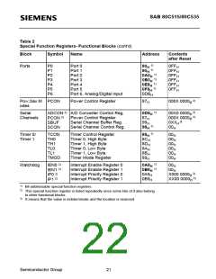
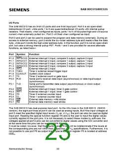
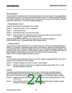
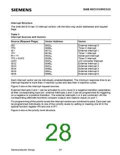
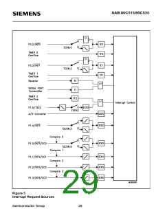
SAB 80C515/80C535
Serial Port
The serial port of the SAB 80C515 enables full duplex communication between microcontrol-
lers or between microcontroller and peripheral devices.
The serial port can operate in 4 modes:
Mode 0: Shift register mode. Serial data enters and exits through R×D. T×D outputs the
shift clock. 8-bits are transmitted/received: 8 data bits (LSB first).
The baud rate is fixed at 1/12 of the oscillator frequency.
Mode 1: 10-bits are transmitted (through R×D) or received (through T×D): a start bit (0),
8 data bits (LSB first), and a stop bit (1). The baud rate is variable.
Mode 2: 11-bits are transmitted (through R×D) or received (through T×D): a start bit (0),
8 data bits (LSB first), a programmable 9th data bit, and a stop bit (1).
The baud rate is programmable to either 1/32 or 1/64 of the oscillator frequency.
Mode 3: 11-bits are transmitted (through T×D) or received (through R×D): a start bit (0),
8 data bits (LSB first), a programmable 9th data bit, and a stop bit (1). Mode 3
is identical to mode 2 except for the baud rate. The baud rate in mode 3 is variable.
The variable baud rates in modes 1 and 3 can be generated by timer 1 or an internal
baud rate generator.
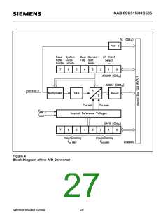
A/D Converter
The 8-bit A/D converter of the SAB 80C515 has eight multiplexed analog inputs (Port 6) and
uses the successive approximation method.
There are three characteristic time frames in a conversion cycle (see A/D converter
characteristics): the conversion time tC, which is the time required for one conversion; the
sample time t which is included in the conversion time and is measured from the start of the
S
conversion; the load time t , which in turn is part of the sample time and also is measured from
L
the conversion start.
Within the load time t , the analog input capacitance C must be loaded to the analog inpult
L
I
voltage level. For the rest of the sample time t , after the load time has passed, the selected
S
analog input must be held constant. During the rest of the conversion time t the conversion
C
itself is actually performed. Conversion can be programmed to be single or continuous; at the
end of a conversion an interrupt can be generated.
A unique feature is the capability of internal reference voltage programming. The internal
reference voltages V
and V
for the A/D converter both are programmable to one
IntAREF
IntAGND
of 16 steps with respect to the external reference voltages. This feature permits a conversion
with a smaller internal reference voltage range to gain a higher resolution.
In addition, the internal reference voltages can easily be adapted by software to the desired
analog input voltage range.
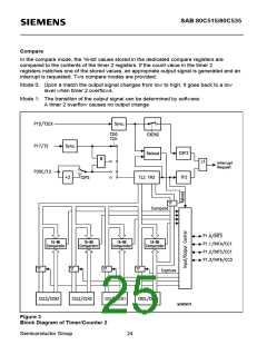
Figure 4 shows a block diagram of the A/D converter.
Semiconductor Group
25

 INFINEON [ Infineon ]