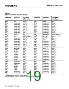
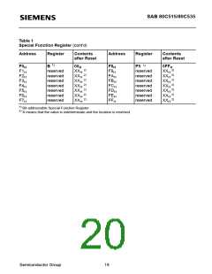
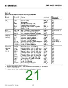
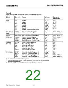
SAB 80C515/80C535
I/O Ports
The SAB 80C515 has six 8-bit I/O ports and one 8-bit input port. Port 0 is an open-drain
bidirectional I/O port, while ports 1 to 5 are quasi-bidirectional I/O ports with internal pullup
resistors. That means, when configured as inputs, ports 1 to 5 will be pulled high and will source
current when externally pulled low. Port 0 will float when configured as input.
Port 0 and port 2 can be used to expand the program and data memory externally. During an
access to external memory, port 0 emits the low-order address byte and reads/writes the data
byte, while port 2 emits the high-order address byte. In this function, port 0 is not an open-drain
port, but uses a strong internal pullup FET. Ports 1 and 3 are provided for several alternate
functions, as listed below:
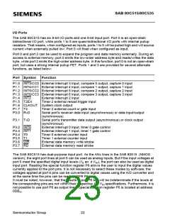
Port Symbol
Function
P1.0 INT3/CC0 External interrupt 3 input, compare 0 output, capture 0 input
P1.1 INT4/CC1 External interrupt 4 input, compare 1 output, capture 1 input
P1.2 INT5/CC2 External interrupt 5 input, compare 2 output, capture 2 input
P1.3 INT6/CC3 External interrupt 6 input, compare 3 output, capture 3 input
P1.4 INT2
P1.5 T2EX
External interrupt 2 input
Timer 2 external reload trigger input
P1.6 CLKOUT System clock output
P1.7 T2
Timer 2 external count or gate input
P3.0 R×D
Serial port’s receiver data input (asynchronous) or data input/output
(synchronous)
P3.1 T×D
Serial port’s transmitter data output (asynchronous) or clock output
(synchronous)
P3.2 INT0
P3.3 INT1
P3.4 T0
External interrupt 0 input, timer 0 gate control
External interrupt 1 input, timer 1 gate control
Timer 0 external counter input
P3.5 T1
Timer 1 external counter input
P3.6 WR
P3.7 RD
External data memory write strobe
External data memory read strobe
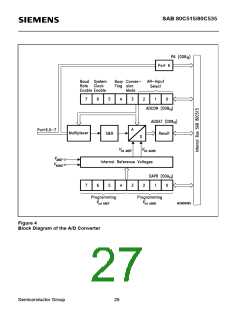
The SAB 80C515 has dual-purpose input port. As the ANx lines in the SAB 80515 (NMOS
version), the eight port lines at port 6 can be used as analog inputs. But if the input voltages at
port 6 meet the specified digital input levels (V an d V ), the port can also be used as digital
IL
IH
input port. Reading the special function register P6 allows the user to input the digital values
currently applied to the port pins. It is not necessary to select these modes by software; the
voltages applied at port 6 pins can be converted to digital values using the A/D converter and
at the same time the pins can be read via SFR P6.
It must be noted, however, that the results in port P6 bits will be indeterminate if the levels at
the corresponding pins are not within their respective V /V specifications. Furthermore, it is
IL IH
not possible to use port P6 as output lines. Special function register P6 is located at address
0DB .
H
Semiconductor Group
22

 INFINEON [ Infineon ]