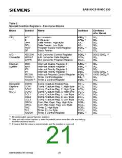
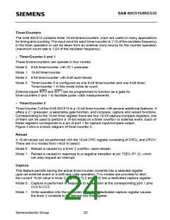
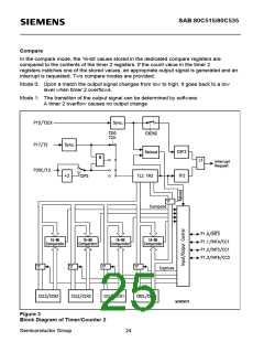
SAB 80C515/80C535
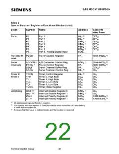
Table 2
Special Function Registers- Functional Blocks (cont’d)
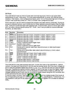
Block
Symbol
Name
Address
Contents
after Reset
1)
1)
Ports
P0
P1
P2
P3
P4
P5
P6
Port 0
Port 1
Port 2
Port 3
Port 4
Port 5
80
90
0A0
0B0
0E8
0F8
0DB
0FF
0FF
0FF
0FF
0FF
0FF
H
H
H
H
H
H
H
H
1)
1)
1)
1)
H
H
H
H
Port 6, Analog/Digital Input
H
2)
Pow.Sav.M PCON
odes
Power Control Register
87
000X 0000
H
B
1)
2)
2)
ADCON 2)
PCON 2)
SBUF
Serial
Channels
A/D Converter Control Reg.
Power Control Register
Serial Channel Buffer Reg.
Serial Channel Control Reg.
0D8
00X0 0000
000X 0000
H
B
B
87
99
98
H
H
H
3)
0XX
H
1)
1)
00
SCON
H
Timer 0/
Timer 1
TCON
TH0
TH1
TL0
TL1
Timer Control Register
Timer 0, High Byte
Timer 1, High Byte
Timer 0, Low Byte
Timer 1, Low Byte
Timer Mode Register
88
00
00
00
00
00
00
H
H
H
H
H
H
H
8C
8D
H
H
H
H
H
8A
8B
89
TMOD
1)
1)
IEN0 2)
IEN1 2)
IP0 2)
Watchdog
Interrupt Enable Register 0
Interrupt Enable Register 1
Interrupt Priority Register 0
Interrupt Priority Register 1
0A8
0B8
0A9
00
00
H
H
H
H
2)
3)
X000 0000
XX00 0000
H
H
B
IP1 2)
0B9
B
1)
Bit-addressable special function registers
This special function register is listed repeatedly since some bits of it also belong
to other functional blocks.
2)
3)
X means that the value is indeterminate and the location is reserved
Semiconductor Group
21

 INFINEON [ Infineon ]