S29GL01GP
S29GL512P
S29GL256P
S29GL128P
7.7.7
Accelerated Program
Accelerated single word programming and write buffer programming operations are enabled through the WP#/ACC pin. This method
is faster than the standard program command sequences.
Note
The accelerated program functions must not be used more than 10 times per sector.
If the system asserts VHH on this input, the device automatically enters the aforementioned Unlock Bypass mode and uses the
higher voltage on the input to reduce the time required for program operations. The system can then use the Write Buffer Load
command sequence provided by the Unlock Bypass mode. Note that if a “Write-to-Buffer-Abort Reset” is required while in Unlock
Bypass mode, the full 3-cycle RESET command sequence must be used to reset the device. Removing VHH from the ACC input,
upon completion of the embedded program operation, returns the device to normal operation.
Sectors must be unlocked prior to raising WP#/ACC to VHH
.
The WP#/ACC pin must not be at VHH for operations other than accelerated programming, or device damage may result.
It is recommended that WP#/ACC apply VHH after power-up sequence is completed. In addition, it is recommended that WP#/
ACC apply from VHH to VIH/VIL before powering down VCC/VIO.
7.7.8
Unlock Bypass
This device features an Unlock Bypass mode to facilitate shorter programming commands. Once the device enters the Unlock
Bypass mode, only two write cycles are required to program data, instead of the normal four cycles.
This mode dispenses with the initial two unlock cycles required in the standard program command sequence, resulting in faster total
programming time. The Command Definitions on page 64 shows the requirements for the unlock bypass command sequences.
During the unlock bypass mode, only the Read, Program, Write Buffer Programming, Write-to-Buffer-Abort Reset, Unlock Bypass
Sector Erase, Unlock Bypass Chip Erase and Unlock Bypass Reset commands are valid. To exit the unlock bypass mode, the
system must issue the two-cycle unlock bypass reset command sequence. The first cycle address is “don't care” and the data 90h.
The second cycle need only contain the data 00h. The sector then returns to the read mode.
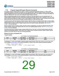
Software Functions and Sample Code
The following are C source code examples of using the unlock bypass entry, program, and exit functions. Refer to the Cypress Low
Level Driver User’s Guide (available soon on www.cypress.com) for general information on Cypress Flash memory software
development guidelines.
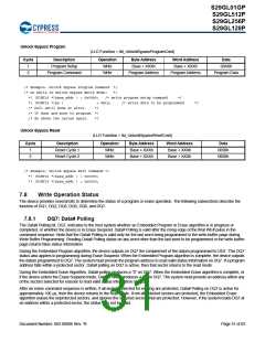
Unlock Bypass Entry
(LLD Function = lld_UnlockBypassEntryCmd)
Cycle
Description
Unlock
Operation
Write
Byte Address
Base + AAAh
Base + 555h
Base + AAAh
Word Address
Base + 555h
Base + 2AAh
Base + 555h
Data
00AAh
0055h
0020h
1
2
3
Unlock
Write
Entry Command
Write
/* Example: Unlock Bypass Entry Command
*/
*( (UINT16 *)base_addr + 0x555 ) = 0x00AA;
*( (UINT16 *)base_addr + 0x2AA ) = 0x0055;
*( (UINT16 *)base_addr + 0x555 ) = 0x0020;
/* write unlock cycle 1
/* write unlock cycle 2
*/
*/
/* write unlock bypass command
*/
/* At this point, programming only takes two write cycles.
/* Once you enter Unlock Bypass Mode, do a series of like
/* operations (programming or sector erase) and then exit
/* Unlock Bypass Mode before beginning a different type of
/* operations.
*/
*/
*/
*/
*/
Document Number: 002-00886 Rev. *B
Page 30 of 83

 INFINEON [ Infineon ]