CoolSET®-F3R
ICE3BR0665JF
Functional Description
losses present due to the connection of the Startup Cell
to the Drain voltage. To avoid uncontrolled ringing at
switch-on a hysteresis start up voltage is implemented.
The switch-off of the controller can only take place after
Active Mode was entered and VVCC falls below 10.5V.
The maximum current consumption before the
controller is activated is about 150µA.
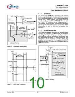
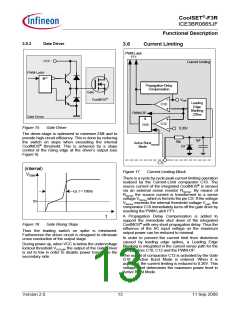
Amplified Current Signal
FB
When VVCC falls below the off-threshold VCCoff=10.5V,
the bias circuit is switched off and the soft start counter
is reset. Thus it is ensured that at every startup cycle
the soft start starts at zero.
The internal bias circuit is switched off if Auto Restart
Mode is entered. The current consumption is then
reduced to 250µA.
Once the malfunction condition is removed, this block
will then turn back on. The recovery from Auto Restart
Mode does not require re-cycling the AC line.
When Active Burst Mode is entered, the internal Bias is
switched off most of the time in order to reduce the
current consumption below 500µA.
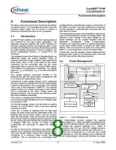
0.68V
Driver
t
t
ton
Figure 5
Pulse Width Modulation
3.3
Improved Current Mode
Soft-Start Comparator
In case the amplified current sense signal exceeds the
FB signal the on-time ton of the driver is finished by
resetting the PWM-Latch (see Figure 5).
The primary current is sensed by the external series
resistor RSense inserted in the source of the integrated
CoolMOS®. By means of Current Mode regulation, the
secondary output voltage is insensitive to the line
variations. The current waveform slope will change with
the line variation, which controls the duty cycle.
The external RSense allows an individual adjustment of
the maximum source current of the integrated
CoolMOS®.
PWM-Latch
FB
R
Q
C8
Driver
S
Q
To improve the Current Mode during light load
conditions the amplified current ramp of the PWM-OP
is superimposed on a voltage ramp, which is built by
the switch T2, the voltage source V1 and a resistor R1
(see Figure 6). Every time the oscillator shuts down for
maximum duty cycle limitation the switch T2 is closed
by VOSC. When the oscillator triggers the Gate Driver,
T2 is opened so that the voltage ramp can start.
In case of light load the amplified current ramp is too
small to ensure a stable regulation. In that case the
Voltage Ramp is a well defined signal for the
comparison with the FB-signal. The duty cycle is then
controlled by the slope of the Voltage Ramp.
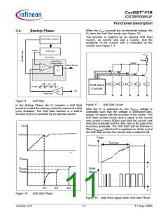
By means of the time delay circuit which is triggered by
the inverted VOSC signal, the Gate Driver is switched-off
until it reaches approximately 156ns delay time (see
Figure 7). It allows the duty cycle to be reduced
continuously till 0% by decreasing VFB below that
threshold.
0.68V
PWM OP
x3.3
CS
Improved
Current Mode
Figure 4
Current Mode
Current Mode means the duty cycle is controlled by the
slope of the primary current. This is done by comparing
the FB signal with the amplified current sense signal.
Version 2.0
9
11 Sep 2008

 INFINEON [ Infineon ]