CoolSET®-F3R
ICE3BR0665JF
Functional Description
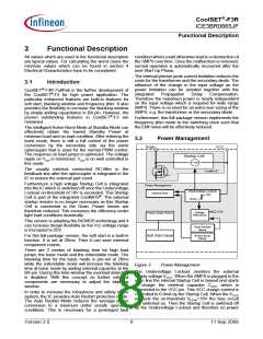
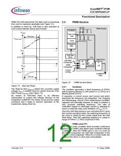
3.3.1
PWM-OP
The input of the PWM-OP is applied over the internal
Soft-Start Comparator
PWM Comparator
leading edge blanking to the external sense resistor
R
Sense connected to pin CS. RSense converts the source
current into a sense voltage. The sense voltage is
amplified with a gain of 3.3 by PWM OP. The output of
the PWM-OP is connected to the voltage source V1.
The voltage ramp with the superimposed amplified
current signal is fed into the positive inputs of the PWM-
Comparator C8 and the Soft-Start-Comparator (see
Figure 6).
FB
C8
PWM-Latch
Oscillator
VOSC
time delay
circuit (156ns)
Gate Driver
X3.3
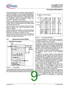
3.3.2
PWM-Comparator
0.68V
10kΩ
The PWM-Comparator compares the sensed current
signal of the integrated CoolMOS® with the feedback
signal VFB (see Figure 8). VFB is created by an external
optocoupler or external transistor in combination with
the internal pull-up resistor RFB and provides the load
information of the feedback circuitry. When the
amplified current signal of the integrated CoolMOS®
exceeds the signal VFB the PWM-Comparator switches
off the Gate Driver.
R1
T2
V1
PWM OP
Voltage Ramp
Figure 6
Improved Current Mode
5V
Soft-Start Comparator
RFB
FB
VOSC
PWM-Latch
C8
max.
Duty Cycle
PWM Comparator
t
Voltage Ramp
0.68V
Optocoupler
PWM OP
0.68V
FB
CS
X3.3
t
Gate Driver
Improved
Current Mode
156ns time delay
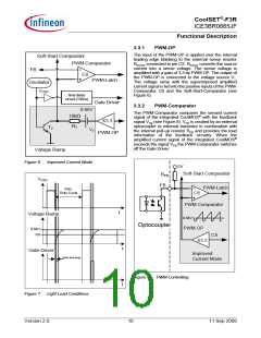
Figure 8
PWM Controlling
t
Figure 7
Light Load Conditions
Version 2.0
10
11 Sep 2008

 INFINEON [ Infineon ]