F3
ICE3AS02 / ICE3AS02G / ICE3BS02 / ICE3BS02G
Electrical Characteristics
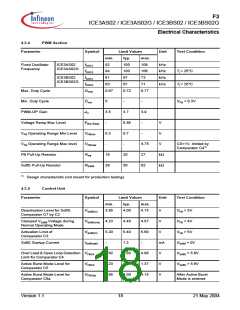
4.3.4
PWM Section
Parameter
Symbol
Limit Values
Unit
Test Condition
min.
92
typ.
100
100
67
max.
Fixed Oscillator
Frequency
ICE3AS02
ICE3AS02G
fOSC1
fOSC2
fOSC1
fOSC2
Dmax
108
106
73
kHz
kHz
kHz
kHz
94
Tj = 25°C
Tj = 25°C
ICE3BS02
ICE3BS02G
61
63
67
71
Max. Duty Cycle
Min. Duty Cycle
PWM-OP Gain
0.67
0.72
0.77
Dmin
0
-
-
VFB < 0.3V
AV
3.5
-
3.7
0.85
0.7
-
3.9
-
Voltage Ramp Max Level
VFB Operating Range Min Level
VFB Operating Range Max level
FB Pull-Up Resistor
VMax-Ramp
VFBmin
VFBmax
RFB
V
0.3
-
-
V
4.75
27
62
V
CS=1V, limited by
Comparator C41)
16
39
20
50
kΩ
kΩ
SoftS Pull-Up Resistor
RSoftS
1)
Design characteristic (not meant for production testing)
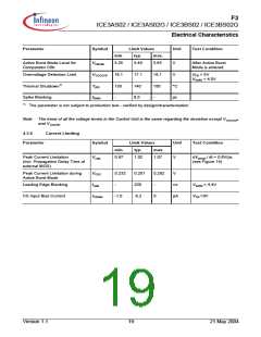
4.3.5
Parameter
Control Unit
Symbol
Limit Values
Unit
Test Condition
min.
typ.
max.
Deactivation Level for SoftS
Comparator C7 by C2
VSoftSC2
3.85
4.00
4.15
V
VFB > 5V
Clamped VSoftS Voltage during
Normal Operating Mode
VSoftSclmp 4.23
4.40
5.40
1.3
4.57
5.60
-
V
VFB = 4V
Activation Limit of
Comparator C3
VSoftSC3
ISoftSstart
5.20
-
V
VFB > 5V
SoftS Startup Current
mA
V
VSoftS = 0V
VSoftS > 5.6V
VSoftS > 5.6V
Over Load & Open Loop Detection VFBC4
Limit for Comparator C4
4.62
1.23
3.85
4.80
1.30
4.00
4.98
1.37
4.15
Active Burst Mode Level for
Comparator C5
VFBC5
V
Active Burst Mode Level for
Comparator C6a
VFBC6a
V
After Active Burst
Mode is entered
Version 1.1
18
21 May 2004

 INFINEON [ Infineon ]