F3
ICE3AS02 / ICE3AS02G / ICE3BS02 / ICE3BS02G
Functional Description
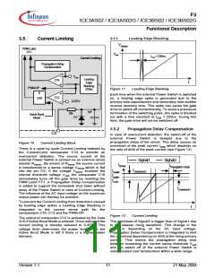
3.5.1
Leading Edge Blanking
3.5
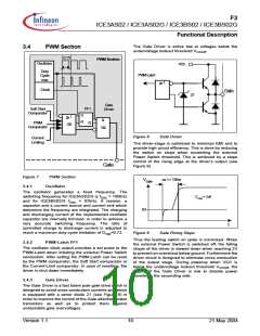
Current Limiting
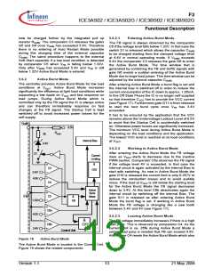
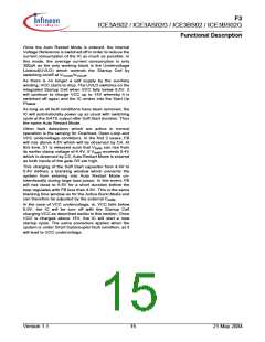
VSense
PWM Latch
FF1
Vcsth
tLEB = 220ns
Current Limiting
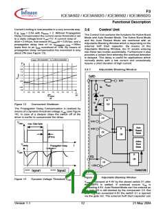
Propagation-Delay
Compensation
Vcsth
Leading
Edge
C10
t
Blanking
220ns
PWM-OP
Figure 11
Leading Edge Blanking
&
Each time when the external Power Switch is switched
on, a leading edge spike is generated due to the
primary-side capacitances and secondary-side rectifier
reverse recovery time. This spike can cause the gate
drive to switch off unintentionally. To avoid a premature
termination of the switching pulse, this spike is blanked
out with a time constant of tLEB = 220ns. During this
time, the gate drive will not be switched off.
C12
G10
0.257V
1pF
10k
Active Burst
Mode
D1
3.5.2
Propagation Delay Compensation
CS
In case of overcurrent detection, the switch-off of the
external Power Switch is delayed due to the
propagation delay of the circuit. This delay causes an
overshoot of the peak current Ipeak which depends on
the ratio of dI/dt of the peak current (see Figure 12).
Figure 10
Current Limiting Block
There is a cycle by cycle Current Limiting realized by
the Current-Limit comparator C10 to provide an
overcurrent detection. The source current of the
external Power Switch is sensed via an external sense
resistor RSense . By means of RSense the source current
is transformed to a sense voltage VSense which is fed
into the pin CS. If the voltage VSense exceeds the
internal threshold voltage Vcsth the comparator C10
immediately turns off the gate drive by resetting the
PWM Latch FF1. A Propagation Delay Compensation
is added to support the immediate shut down without
delay of the Power Switch in case of Current Limiting.
The influence of the AC input voltage on the maximum
output power can thereby be avoided.
Signal1
IOvershoot2
Signal2
tPropagation Delay
ISense
Ipeak2
Ipeak1
ILimit
IOvershoot1
To prevent the Current Limiting from distortions caused
by leading edge spikes a Leading Edge Blanking is
integrated in the current sense path for the
comparators C10, C12 and the PWM-OP.
t
Figure 12
Current Limiting
The output of comparator C12 is activated by the Gate
G10 if Active Burst Mode is entered. Once activated the The overshoot of Signal2 is bigger than of Signal1 due
current limiting is thereby reduced to 0.257V. This to the steeper rising waveform. This change in the
voltage level determines the power level when the slope is depending on the AC input voltage.
Active Burst Mode is left if there is a higher power Propagation Delay Compensation is integrated to limit
demand.
the overshoot dependency on dI/dt of the rising primary
current. That means the propagation delay time
between exceeding the current sense threshold Vcsth
and the switch off of the external Power Switch is
compensated over temperature within a wide range.
Version 1.1
11
21 May 2004

 INFINEON [ Infineon ]