CoolSET®-F3R
ICE3BR4765J
Functional Description
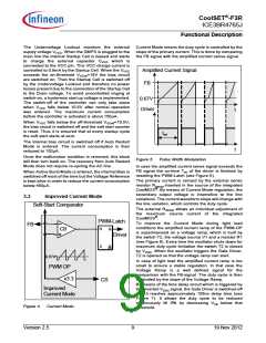
3.5.3
Gate Driver
3.6
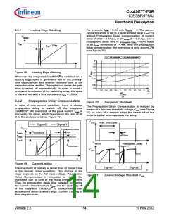
Current Limiting
PWM Latch
FF1
VCC
Current Limiting
PWM-Latch
1
Propagation-Delay
Compensation
Gate
CoolMOS®
Vcsth
Leading
Edge
C10
Blanking
220ns
PWM-OP
Gate Driver
&
C12
G10
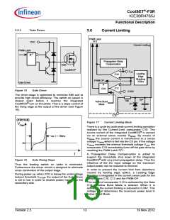
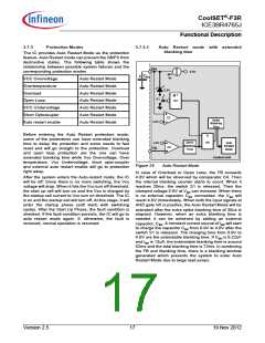
Figure 15
Gate Driver
0.34V
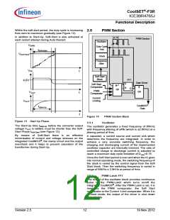
The driver-stage is optimized to minimize EMI and to
provide high circuit efficiency. The switch on speed is
slowed down before it reaches the integrated
CoolMOS® turn on threshold. That is a slope control of
the rising edge at the output of the driver (see Figure
16).
1pF
10k
Active Burst
Mode
D1
CS
(internal)
VGate
Figure 17
Current Limiting Block
There is a cycle by cycle peak current limiting operation
realized by the Current-Limit comparator C10. The
source current of the integrated CoolMOS® is sensed
via an external sense resistor RSense. By means of
RSense the source current is transformed to a sense
voltage VSense which is fed into the CS pin. If the voltage
ca. t = 130ns
5V
VSense exceeds the internal threshold voltage Vcsth, the
comparator C10 immediately turns off the gate drive by
resetting the PWM Latch FF1.
A
Propagation Delay Compensation is added to
t
support the immediate shut down of the integrated
CoolMOS® with very short propagation delay. Thus the
influence of the AC input voltage on the maximum
output power can be reduced to minimal.
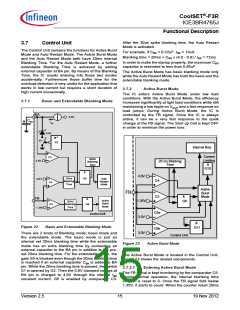
Figure 16
Gate Rising Slope
Thus the leading switch on spike is minimized.
Furthermore the driver circuit is designed to eliminate
cross conduction of the output stage.
In order to prevent the current limit from distortions
caused by leading edge spikes,
Blanking is integrated in the current sense path for the
comparators C10, C12 and the PWM-OP.
a Leading Edge
During power up, when VCC is below the undervoltage
lockout threshold VVCCoff, the output of the Gate Driver
is set to low in order to disable power transfer to the
secondary side.
The output of comparator C12 is activated by the Gate
G10 if Active Burst Mode is entered. When it is
activated, the current limiting is reduced to 0.34V. This
voltage level determines the maximum power level in
Active Burst Mode.
Version 2.5
13
19 Nov 2012

 INFINEON [ Infineon ]