CoolSET®-F3R
ICE3BR4765J
Functional Description
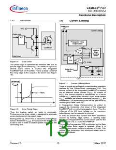
3.6.1
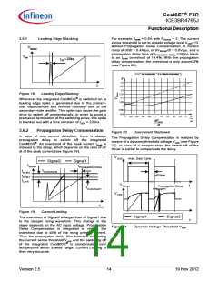
Leading Edge Blanking
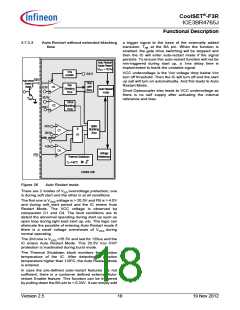
For example, Ipeak = 0.5A with RSense = 2. The current
sense threshold is set to a static voltage level Vcsth=1V
without Propagation Delay Compensation. A current
ramp of dI/dt = 0.4A/µs, or dVSense/dt = 0.8V/µs, and a
propagation delay time of tPropagation Delay =180ns leads
to an Ipeak overshoot of 14.4%. With the propagation
delay compensation, the overshoot is only around 2%
(see Figure 20).
VSense
Vcsth
tLEB = 220ns
with compensation
without compensation
V
1,3
1,25
1,2
t
Figure 18
Leading Edge Blanking
1,15
1,1
Whenever the integrated CoolMOS® is switched on, a
leading edge spike is generated due to the primary-
side capacitances and reverse recovery time of the
secondary-side rectifier. This spike can cause the gate
drive to switch off unintentionally. In order to avoid a
premature termination of the switching pulse, this spike
is blanked out with a time constant of tLEB = 220ns.
1,05
1
0,95
0,9
0
0,2
0,4
0,6
0,8
1
1,2
1,4
1,6
1,8
2
V
dVSense
dt
μs
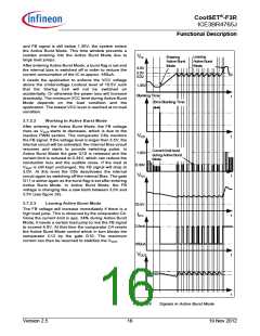
3.6.2
Propagation Delay Compensation
Figure 20
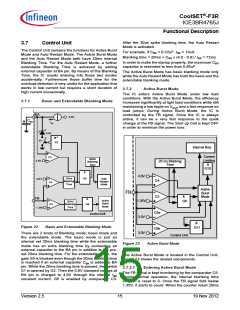
Overcurrent Shutdown
In case of over-current detection, there is always
propagation delay to switch off the integrated
CoolMOS®. An overshoot of the peak current Ipeak is
induced to the delay, which depends on the ratio of dI/
dt of the peak current (see Figure 19).
The Propagation Delay Compensation is realized by
means of a dynamic threshold voltage Vcsth (see Figure
21). In case of a steeper slope the switch off of the
driver is earlier to compensate the delay.
VOSC
max. Duty Cycle
Signal2
IOvershoot2
Signal1
tPropagation Delay
ISense
Ipeak2
Ipeak1
ILimit
off time
VSense
t
Propagation Delay
IOvershoot1
Vcsth
t
Figure 19
Current Limiting
Signal1
Signal2
The overshoot of Signal2 is larger than of Signal1 due
to the steeper rising waveform. This change in the
slope depends on the AC input voltage. Propagation
Delay Compensation is integrated to reduce the
overshoot due to dI/dt of the rising primary current.
Thus the propagation delay time between exceeding
the current sense threshold Vcsth and the switching off
of the integrated CoolMOS® is compensated over
temperature within a wide range. Current Limiting is
then very accurate.
t
Figure 21
Dynamic Voltage Threshold Vcsth
Version 2.5
14
19 Nov 2012

 INFINEON [ Infineon ]