CoolSET™-F2
ICE2A165/265/365
ICE2A180/280
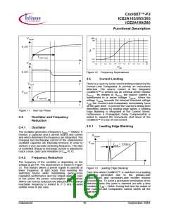
Functional Description
The primary current is sensed by the external series
resistor RSense inserted in the source of the integrated
CoolMOS™. By means of Current Mode the regulation
of the secondary voltage is insensitive on line
variations. Line variation causes varition of the
increasing current slope which controls the duty cycle.
The external RSense allows an individual adjustment of
the maximum source current of the integrated
CoolMOS™.
VO SC
m ax.
Duty Cycle
Voltage Ram p
t
Soft-Start Com parator
PW M Com parator
FB
0.8V
FB
0.3V
PW M -Latch
Gate Driver
t
0.3V
Oscillator
C5
Gate Driver
VO SC
0.8V
10k
Ω
x3.65
t
R1
T2
V1
PW M OP
Figure 7
Light Load Conditions
C1
20pF
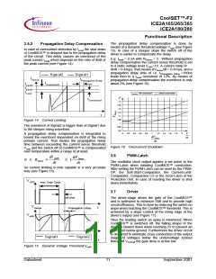
3.2.1
PWM-OP
Voltage Ramp
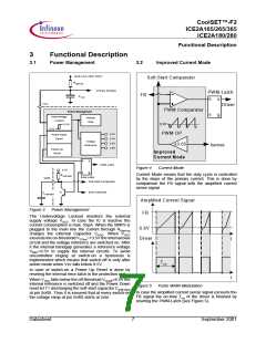
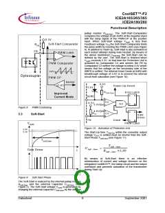
Figure 6 Improved Current Mode
The input of the PWM-OP is applied over the internal
leading edge blanking to the external sense resistor
RSense connected to pin ISense. RSense converts the
source current into a sense voltage. The sense voltage
is amplified with a gain of 3.65 by PWM OP. The output
of the PWM-OP is connected to the voltage source V1.
The voltage ramp with the superimposed amplified
current singal is fed into the positive inputs of the PWM-
Comparator, C5 and the Soft-Start-Comparator.
To improve the Current Mode during light load
conditions the amplified current ramp of the PWM-OP
is superimposed on a voltage ramp, which is built by
the switch T2, the voltage source V1 and the 1st order
low pass filter composed of R1 and C1(see Figure 6,
Figure 7). Every time the oscillator shuts down for max.
duty cycle limitation the switch T2 is closed by VOSC
When the oscillator triggers the Gate Driver T2 is
opened so that the voltage ramp can start.
.
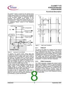
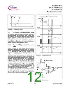
3.2.2
PWM-Comparator
The PWM-Comparator compares the sensed current
signal of the integrated CoolMOSTM with the feedback
signal VFB (see Figure 8). VFB is created by an external
optocoupler or external transistor in combination with
the internal pullup resistor RFB and provides the load
information of the feedback circuitry. When the
amplified current signal of the integrated CoolMOS™
exceeds the signal VFB the PWM-Comparator switches
off the Gate Driver.
In case of light load the amplified current ramp is to
small to ensure a stable regulation. In that case the
Voltage Ramp is a well defined signal for the
comparison with the FB-signal. The duty cycle is then
controlled by the slope of the Voltage Ramp.
By means of the C5 Comparator the Gate Driver is
switched-off until the voltage ramp exceeds 0.3V. It
allows the duty cycle to be reduced continously till 0%
by decreasing VFB below that threshold.
Datasheet
8
September 2001

 INFINEON [ Infineon ]