CoolSET™-F2
ICE2A165/265/365
ICE2A180/280
Functional Description
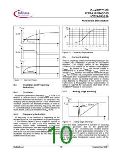
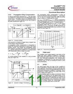
The propagation delay compensation is done by
means of a dynamic threshold voltage Vcsth (see Figure
15). In case of a steeper slope the switch off of the
driver is earlier to compensate the delay.
3.5.2
Propagation Delay Compensation
In case of overcurrent detection by ILimit the shut down
of CoolMOS™ is delayed due to the propagation delay
of the circuit. This delay causes an overshoot of the
peak current Ipeak which depends on the ratio of dI/dt of
the peak current (see Figure 14).
E.g. Ipeak = 0.5A with RSense = 2 . Without propagation
delay compensation the current sense threshold is set
to a static voltage level Vcsth=1V. A current ramp of
dI/dt = 0.4A/µs, that means dVSense/dt = 0.8V/µs, and a
propagation delay time of i.e. tPropagation Delay =180ns
leads then to a Ipeak overshoot of 12%. By means of
propagation delay compensation the overshoot is only
about 2% (see Figure 16).
.
Signal2
IO vershoot2
Signal1
tPropagation Delay
ISense
Ipeak2
Ipeak1
ILim it
with compensation
without compensation
V
1,3
IO vershoot1
1,25
1,2
1,15
1,1
t
1,05
1
Figure 14 Current Limiting
The overshoot of Signal2 is bigger than of Signal1 due
to the steeper rising waveform.
0,95
0,9
0
0,2 0,4 0,6 0,8
1
1,2 1,4 1,6 1,8
2
V
A propagation delay compensation is integrated to
bound the overshoot dependent on dI/dt of the rising
primary current. That means the propagation delay
time between exceeding the current sense threshold
dVSense
dt
µs
Figure 16 Overcurrent Shutdown
Vcsth and the switch off of CoolMOS™ is compensated
over temperature within a range of at least.
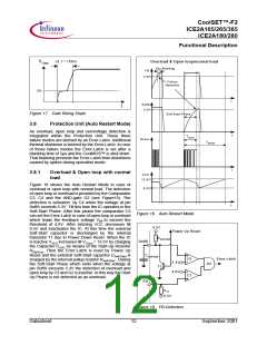
3.6
PWM-Latch
dI
dV Sense
dt
peak
0 ≤ RSense
×
≤ 1
The oscillator clock output applies a set pulse to the
PWM-Latch when initiating CoolMOS™ conduction.
After setting the PWM-Latch can be reset by the PWM-
OP, the Soft-Start-Comparator, the Current-Limit-
Comparator, Comparator C3 or the Error-Latch of the
Protection Unit. In case of reseting the driver is shut
down immediately.
dt
So current limiting is now capable in a very accurate
way (see Figure 16).
VOSC
max. Duty Cycle
3.7
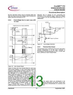
Driver
off time
The driver-stage drives the gate of the CoolMOS™
and is optimized to minimize EMI and to provide high
circuit efficiency. This is done by reducing the switch on
slope when reaching the CoolMOS™ threshold. This is
achieved by a slope control of the rising edge at the
driver’s output (see Figure 17).
VSense
t
Propagation Delay
Vcsth
Thus the leading switch on spike is minimized. When
CoolMOS™ is switched off, the falling shape of the
driver is slowed down when reaching 2V to prevent an
overshoot below ground. Furthermore the driver circuit
is designed to eliminate cross conduction of the output
stage. At voltages below the undervoltage lockout
threshold VVCCoff the gate drive is active low.
Signal1
Signal2
t
Figure 15 Dynamic Voltage Threshold Vcsth
Datasheet
11
September 2001

 INFINEON [ Infineon ]