AIROC™ Bluetooth® system on chip for automotive applications
Specifications
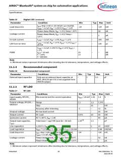
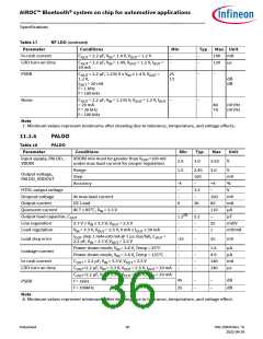
Table 17
RF LDO (continued)
Conditions
COUT = 2.2 μF, VIN = 1.4 V, VOUT = 1.2 V
OUT = 2.2 μF, VIN = 1.4V, VOUT = 1.2 V, IOUT
20 mA
Parameter
In-rush current
LDO turn on time
Min
–
–
Typ
–
–
Max Unit
100 mA
120 μs
C
=
PSRR
C
OUT = 2.2 μF, 1.235 V ≤ VIN ≤ 1.4 V, VOUT
=
25
13
–
–
1.2 V,
dB
dB
IOUT = 20 mA
f = 1 kHz
f = 100 kHz
Noise
C
OUT = 2.2 μF, VIN = 1.235 V, VOUT = 1.2 V, IOUT
–
–
= 20 mA
80
70
nVHz
nVHz
f = 30 kHz
f = 100 kHz
Note
7. Minimum values represent minimums after derating due to tolerance, temperature, and voltage effects.
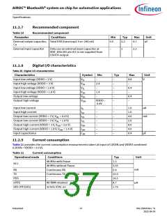
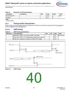
11.2.6
PALDO
Table 18
PALDO
Parameter
Conditions
Min
2.6
Typ
3.0
Max
3.63
3.0
Unit
Input supply, PALDO_- VDDIN min must be greater than VOUT+100 mV
VDDIN
V
under max load current for proper regulation
Range
Step
1.5
2.45
100
–
3.3
–
V
mV
%
Output voltage,
PALDO_VDDOUT
Accuracy
-4
–
–
0
–
+4
–
100
60
110
–
HTOL output voltage
Dropout voltage
Output current
Quiescent current
Output load capacitor, COUT
V
At max load current
DC Load
At T ≤ 85C, VIN = 3.3 V
mV
mA
μA
30
–
1.2[8] 2.2
μF
Line regulation
Load regulation
2.7 V ≤ VIN ≤ 3.3 V, VOUT = 2.5 V
IN = 3.3 V, VOUT = 2.5 V, 0 mA ≤ IOUT ≤ 30 mA
–
–
–
–
25
1
mV/V
mV/mA
V
IOUT step 1 mA20 mA @ 1 s rise/fall, COUT
2.2 F, VIN = 3.3 V, VOUT = 2.5 V
Power-down mode, VIN = 3.6 V, Temp = 25C
Power-down mode, VIN = 3.6 V, Temp = 125C
=
Load step error
Leakage current
-25
–
25
mV
–
–
–
–
–
–
–
–
1.6
4.9
140
140
μA
μA
mA
μs
In-rush current
LDO turn on time
C
C
OUT = 2.2 F, VIN = 3.3 V, VOUT = 2.5 V
OUT=2.2 F, VIN = 3.3 V, VOUT = 2.5 V, IOUT = 20 mA
COUT=2.2 F, VIN = 3.3 V, VOUT = 2.5 V, IOUT = 20 mA
45
25
–
–
–
–
dB
dB
PSRR
f = 1kHz
f = 100kHz
Note
8. Minimum values represent minimums after derating due to tolerance, temperature, and voltage effect.
Datasheet
36
002-25826 Rev. *G
2022-09-24

 INFINEON [ Infineon ]