AIROC™ Bluetooth® system on chip for automotive applications
Specifications
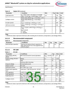
Table 15
Digital LDO (continued)
Condition
Parameter
Min
Typ Max Unit
IOUT step 1 mA 20 mA @ 1 μs rise/fall,
COUT = 2.2 μF, VIN = 1.235 V, VOUT = 1.2V
Power down Mode, VIN = 1.4 V, Temp = 25C –
Power down Mode, VIN = 1.4 V, Temp =
125C
COUT = 2.2 μF, VIN = 1.4 V, VOUT = 1.2 V
COUT = 2.2 μF, VIN = 1.4 V, VOUT = 1.2 V, IOUT
20 mA
Load step error
–24
–
–
–
–
–
+24
50
mV
nA
μA
mA
s
Leakage current
–
2
In-rush current
–
–
100
120
=
LDO turn on time
COUT = 2.2 μF, 1.235 V ≤ VIN ≤ 1.4 V, VOUT
1.2 V,
=
PSRR
IOUT = 20 mA
f = 1 kHz
f = 100 kHz
25
13
–
–
dB
dB
Note
6. Minimum values represent minimums after derating due to tolerance, temperature, and voltage effects.
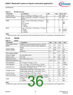
11.2.4
Recommended component
Table 16
Recommended component
Conditions
Parameter
Min
–
Typ
1
Max
2.2
Unit
μF
External input capacitor
Only use an external input capacitor at
VDD_DIGLDO pin if it is not supplied from
CBUCK output.
11.2.5
RF LDO
Table 17
RF LDO
Parameter
Conditions
Min
Typ
Max Unit
Input supply, RFLDO_-
VDDIN
Min must be met for correct operation
VOUT + 20 mV 1.26 1.4
V
Output voltage, RFLDO_- Range
1.1
–
–2
–
0.075
–
1.55[7]
1.2
25
–
–
20
–
1.275
–
VDDOUT
Step
mV
%
mV
mA
μA
μF
Accuracy after trimming
+2
20
60
40
–
Dropout voltage
Output current
Quiescent current
Output load capacitor,
COUT
At max load current
DC Load
At T ≤ 85C, VIN = 1.4V
Total trace + cap ESR must be < 80 mΩ
2.2
Line regulation
Load regulation
Load step error
1.235 V ≤ VIN ≤ 1.4 V
–
5
–
–
10
mV/V
VOUT = 1.2 V, VIN = 1.26 V, 1 mA ≤ IOUT ≤ 25 mA –
0.44 mV/mA
+24 mV
I
OUT step 1 mA 20 mA @ 1 μs rise/fall,
–24
COUT = 2.2 μF, VIN = 1.235 V, VOUT = 1.2 V
Leakage current
Power down mode, VIN = 1.4 V, Temp = 25C
Power down mode, VIN = 1.4 V, Temp = 125C –
–
–
–
50
2
nA
μA
Note
7. Minimum values represent minimums after derating due to tolerance, temperature, and voltage effects.
Datasheet
35
002-25826 Rev. *G
2022-09-24

 INFINEON [ Infineon ]