BTS 611 L1
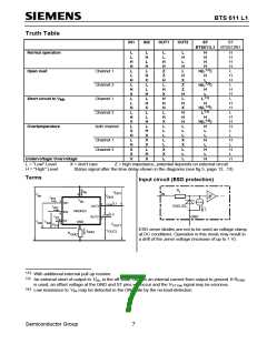
Truth Table
IN1
IN2
OUT1
OUT2
ST
ST
BTS611L1 BTS612N1
Normal operation
Open load
L
L
H
H
L
L
H
L
H
X
L
L
H
L
H
X
L
X
H
L
H
X
X
X
L
H
L
H
L
H
X
L
L
H
L
H
X
L
L
H
L
H
X
X
X
L
H
X
L
L
H
H
Z
Z
H
L
H
X
H
H
H
L
H
X
L
L
L
L
L
X
X
L
L
H
L
H
L
H
X
Z
Z
H
L
H
X
H
H
H
L
L
L
X
X
L
L
L
H
H
H
H
H
H
H
H
L
H
H
L
H
H
L
H
H
L
H
H
H
L
L
H
L
12)
Channel 1
Channel 2
Channel 1
Channel 2
both channel
H(L
)
)
H
L
12)
H(L
H
L
13)
Short circuit to V
Overtemperature
L
bb
H
14)
13)
H(L
L
)
H
14)
H(L
)
H
L
L
H
L
H
L
H
Channel 1
Channel 2
H
L
H
Undervoltage/ Overvoltage
L = "Low" Level
H = "High" Level
X = don't care
Z = high impedance, potential depends on external circuit
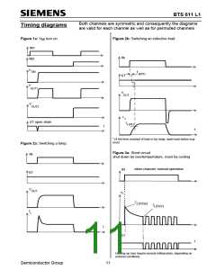
Status signal after the time delay shown in the diagrams (see fig 5. page 12...13)
Terms
Input circuit (ESD protection)
R
I
V
bb
I
ON1
V
IN
4
V
bb
I
ON2
IN1
V
3
bb
I
IN1
IN2
ST
L1
1
7
OUT1
OUT2
ESD-ZDI
I
IN2
I
I
PROFET
I
6
5
L2
V
I
GND
ST
V
V
GND
2
IN2
IN1
V
ST
OUT1
ESD zener diodes are not to be used as voltage clamp
at DC conditions. Operation in this mode may result in
a drift of the zener voltage (increase of up to 1 V).
V
I
OUT2
GND
R
GND
12)
13)
With additional external pull up resistor
An external short of output to Vbb, in the off state, causes an internal current from output to ground. If RGND
is used, an offset voltage at the GND and ST pins will occur and the VST low signal may be errorious.
Low resistance to Vbb may be detected in the ON-state by the no-load-detection
14)
Semiconductor Group
7

 INFINEON [ Infineon ]